
non-volatile memory

A non-volatile, memory technology, used in static memory, read-only memory, information storage, etc., can solve problems such as increasing the operating voltage, reducing the ratio of high resistance states, and affecting the resistance conversion characteristics of resistive non-volatile memory

Active Publication Date: 2016-08-10
WINBOND ELECTRONICS CORP
View PDF6 Cites 0 Cited by
  • Summary
  • Abstract
  • Description
  • Claims
  • Application Information

AI Technical Summary

Problems solved by technology

However, the above method will affect the resistance conversion characteristics of the resistive non-volatile memory, such as increasing the operating voltage, increasing the operating current, reducing the ratio of high resistance state to low resistance state, etc.

Method used


Image

  • non-volatile memory

Examples


Embodiment Construction

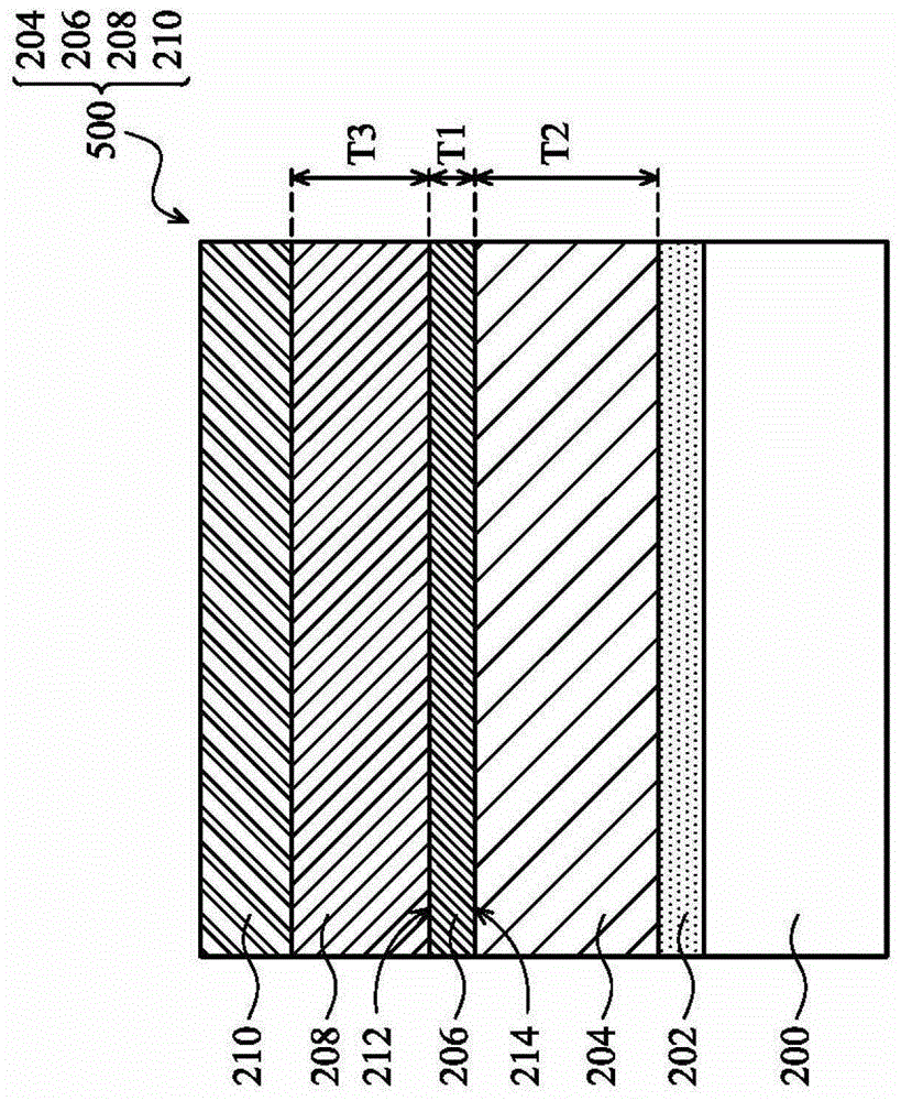
[0018] An embodiment of the present invention provides a non-volatile memory, such as a resistive non-volatile memory, which uses an external bias to change the resistance value of the resistance transition layer of the non-volatile memory to achieve a memory effect. In the non-volatile memory of the embodiment of the present invention, a separation layer is inserted between the bottom electrode and the resistance transition layer, so that the lattice constant of the resistance transition layer of the non-volatile memory formed finally will not be affected by the lower bottom electrode itself. The influence of the lattice constant makes the grain size (grain size) larger. This approach can significantly increase the resistance ratio between the device's high-resistance storage state and its low-resistance storage state.

[0019] figure 1 It is a schematic cross-sectional view of a non-volatile memory 500 according to an embodiment of the present invention. like figure 1 As ...


PUM


Abstract

The invention provides a non-volatile memory. The aforementioned non-volatile memory comprises a bottom electrode which is provided with a first crystal lattice constant; a resistor state conversion layer which is arranged above the aforementioned bottom electrode and provided with a second crystal lattice constant; a top electrode which is arranged on the aforementioned resistor state conversion layer; and a separating layer which is arranged between the aforementioned bottom electrode and the aforementioned resistor state conversion layer and provided with a third crystal lattice constant which is different from the aforementioned first crystal lattice constant and the aforementioned second crystal lattice constant. Crystal grain size variation amount of the resistor state conversion layer on different crystal chips of the same crystal wafer can be reduced so that characteristics of resistor conversion resistance, ratio of the high resistance state to the low resistance state and element durability of elements can be greatly enhanced.

Description

technical field [0001] The present invention relates to a memory element, in particular to a resistive non-volatile memory. Background technique [0002] Resistive non-volatile memory (RRAM) has low power consumption, low operating voltage, short writing and erasing time, long endurance, long storage time, non-destructive reading, multi-state storage, simple manufacturing process and reliability Miniaturization and other advantages, so become the mainstream of emerging non-volatile memory. However, the conventional resistive non-volatile memory (RRAM) produced by semiconductor manufacturing process will cause the grain size of the resistive transition layer between different chips on the same wafer cannot be reduced and has a large amount of variation. For example, the resistance switching (resistive switching, RS) resistance, the ratio of the high resistance state to the low resistance state, and the device durability (endurance) and other characteristics are not good. ...

Claims


Application Information

Patent Timeline
Patent Type & Authority Patents(China)
IPC IPC(8): H01L45/00G11C16/02
Inventor 张文岳
Owner WINBOND ELECTRONICS CORP
Learn More