Method for preparing magnesium diboride superconducting Josephson junction by secondary mask method
A technology for preparing magnesium diboride and thin films, which is applied in the manufacture/processing of superconductor devices, can solve the problems of difficult to prepare superconducting Josephson junctions, connectivity, etc., and achieves the effects of short annealing time, reduced component diffusion, and clear interface
- Summary
- Abstract
- Description
- Claims
- Application Information
AI Technical Summary
Problems solved by technology
Method used
Image
Examples
Embodiment 1
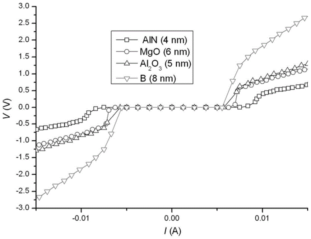
[0052] The preparation of the precursor film in this example was completed in a ZZXS-500 electron beam coating machine, and the electron beam annealing was performed on a self-made EBW-6 electron beam welding machine. The precursor film structure is [Mg(15nm)+B(10nm)] 6 —B(8nm)—[Mg(15nm)+B(10nm)] 5 , the thickness of the precursor film is 283nm, and the size of the substrate SiC is 10.0mm×3.0mm.
[0053] 1. Preparation of precursor film
[0054] (1) Preparation of the underlying precursor film
[0055] (1.1) Fix the SiC bare substrate with a size of 10.0mm×3.0mm on the sample workpiece stage;
[0056] (1.2) Place the sample workpiece table in the ZZXS-500 electron beam coating machine and start vacuuming;
[0057] (1.3) Wait for the vacuum degree to be higher than 5×10 -5 After Pa, turn on the quartz crystal thin film coating controller;
[0058] (1.4) Evaporate layer B on the bare SiC substrate, and the number on the display panel of the quartz crystal thin film coating...
Embodiment 2
[0089] The preparation of the precursor film in this example was completed in a ZZXS-500 electron beam coating machine, and the electron beam annealing was performed on a self-made EBW-6 electron beam welding machine. The precursor film is [Mg(12nm)+B(8nm)] 5 —AlN(4nm)—[Mg(12nm)+B(8nm)] 5 , the thickness of the precursor film is 204nm, and the size of the substrate SiC is 10.0mm×3.0mm.
[0090] 1. Preparation of precursor film
[0091] (1) Preparation of the underlying precursor film
[0092] (1.1) Fix the SiC bare substrate with a size of 10.0mm×3.0mm on the sample workpiece stage;
[0093] (1.2) Place the sample workpiece table in the ZZXS-500 electron beam coating machine and start vacuuming;
[0094] (1.3) Wait for the vacuum degree to be higher than 5×10 -5 After Pa, turn on the quartz crystal thin film coating controller;
[0095] (1.4) Evaporate layer B on the bare SiC substrate, and the number on the display panel of the quartz crystal thin film coating controlle...
Embodiment 3
[0126] The preparation of the precursor film in this example was completed in a ZZXS-500 electron beam coating machine, and the electron beam annealing was performed on a self-made EBW-6 electron beam welding machine. The precursor film is [Mg(12nm)+B(8nm)] 5 —Al 2 o 3 (5nm)—[Mg(15nm)+B(10nm)] 3 , the film thickness is 180nm, and the substrate Si size is 10.0mm×3.0mm.
[0127] 1. Preparation of precursor film
[0128](1) Preparation of the underlying precursor film
[0129] (1.1) Fix the bare Si substrate with a size of 10.0mm×3.0mm on the sample workpiece stage;
[0130] (1.2) Place the sample workpiece table in the ZZXS-500 electron beam coating machine and start vacuuming;
[0131] (1.3) Wait for the vacuum degree to be higher than 5×10 -5 After Pa, turn on the quartz crystal thin film coating controller;
[0132] (1.4) Evaporate layer B on the bare Si substrate, and the number on the display panel of the quartz crystal thin film coating controller is After stop c...
PUM
 Abstract
Description
Claims
Application Information
 - R&D
- Intellectual Property
- Life Sciences
- Materials
- Tech Scout
- Unparalleled Data Quality
- Higher Quality Content
- 60% Fewer Hallucinations
Browse by: Latest US Patents, China's latest patents, Technical Efficacy Thesaurus, Application Domain, Technology Topic, Popular Technical Reports.
© 2025 PatSnap. All rights reserved.Legal|Privacy policy|Modern Slavery Act Transparency Statement|Sitemap|About US| Contact US: help@patsnap.com


