Semiconductor device based on graphene electrode and manufacturing method thereof

A graphene electrode and semiconductor technology, which is applied in the direction of semiconductor devices, electrical components, circuits, etc., can solve problems such as separation or falling off, technical obstacles, and affect device performance, and achieve the effects of graphic optimization, current distribution improvement, and electrical performance improvement

Inactive Publication Date: 2014-07-02
SHANGHAI UNIV
View PDF3 Cites 9 Cited by
  • Summary
  • Abstract
  • Description
  • Claims
  • Application Information

AI Technical Summary

Problems solved by technology

[0003] In recent years, there have been many researches on the use of graphene and its composite materials as electrode materials, and some results have been achieved. However, it should be pointed out that there are still certain technical obstacles in the preparation of high-quality graphene on insulating substrates.
Most of the methods currently used are to prepare graphene or graphene oxide first, and then transfer it to the target substrate by a certain method. The graphene and the substrate are combined by van der Waals force, which is easy to separate or fall off in the subsequent process. , which affects the performance of the device

Method used


Image

  • Semiconductor device based on graphene electrode and manufacturing method thereof
  • Semiconductor device based on graphene electrode and manufacturing method thereof
  • Semiconductor device based on graphene electrode and manufacturing method thereof

Examples


Embodiment 1

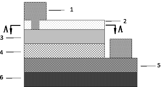
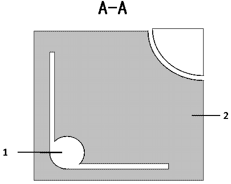
[0022] In this example, see figure 1 and figure 2 , a semiconductor device based on a graphene electrode, which is sequentially formed by combining a substrate layer 6, a first semiconductor layer 5, an active layer 4, a second semiconductor layer 3, and a graphene electrode layer 2, and the reinforcing electrode 1 is made of gold electrode, the substrate layer 6 is sapphire, the first semiconductor layer 5 is N-type gallium nitride, and the second semiconductor layer 3 is P-type gallium nitride, so that the gold electrode is fixedly combined with the graphene electrode layer 2 by pinning and fixing. On the P-type gallium nitride, the graphene electrode layer 2 is penetrated by the gold electrode, and one end of the gold electrode is directly contacted and fixedly connected with the P-type gallium nitride, so that the other end of the gold electrode connects the graphene The electrode layer 2 is pressed and fixed on the P-type gallium nitride, and the gold electrode and the ...

Embodiment 2

[0030] This embodiment is basically the same as Embodiment 1, especially in that:

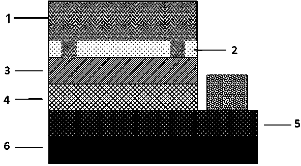
[0031] In this example, see image 3 , a semiconductor device based on a graphene electrode, which is sequentially formed by combining a substrate layer 6, a first semiconductor layer 5, an active layer 4, a second semiconductor layer 3, and a graphene electrode layer 2, and the reinforcing electrode 1 is made of ITO / ZnO Form an ITO / ZnO electrode, the substrate layer 6 is SiC, the first semiconductor layer 5 is N-type gallium nitride, and the second semiconductor layer 3 is P-type gallium nitride, so that the ITO / ZnO electrode is fixed by pinning and bonding the graphene The electrode layer 2 is fixedly combined on the P-type gallium nitride, that is, the graphene electrode layer 2 is penetrated by the ITO / ZnO electrode, and one end of the ITO / ZnO electrode is directly contacted and fixedly connected with the P-type gallium nitride, so that The other end of the ITO / ZnO electrode presses and fi...


PUM


Abstract

The invention discloses a semiconductor device based on a graphene electrode. The semiconductor device based on the graphene electrode is formed by sequentially combining a substrate layer, a first semiconductor layer, an active layer, a second semiconductor layer and a graphene electrode layer. The graphene electrode layer is fixedly combined with the second semiconductor layer through an intensifier electrode in a pining fixing mode, so that materials of the intensifier electrode and graphene materials of the graphene electrode layer are combined mutually into a combination electrode. The invention further discloses a manufacturing method of the semiconductor device based on the graphene electrode. According to the manufacturing method, a graphene film and collaborative conducting materials form the combination electrode, the combination electrode is arranged on a system which is sequentially composed of the substrate, a conductor layer, the active layer and the semiconductor layers, and then a complete device structure is formed. According to the semiconductor device based on the graphene electrode and the manufacturing method of the semiconductor device, the graphene electrode forms the combination structure with pining fixed connection adopted, the adhesion between graphene and the substrate is improved, and the current distribution in the device can be improved through patterning control over the graphene electrode layer.

Description

technical field [0001] The invention relates to a semiconductor device and a preparation process thereof, and also relates to a graphene electrode and a preparation method thereof, which are applied in the technical field of semiconductor device structure and preparation. Background technique [0002] Graphene is a monoatomic layer crystal composed of carbon atoms tightly packed, which has many unique properties, such as high specific surface area, good thermal stability, and excellent thermal conductivity. These excellent properties make graphene have good application prospects in the fields of nanoelectronic devices, gas sensors, supercapacitors and energy storage. In particular, graphene has a very high transmittance in the visible light band and good electrical and thermal transmission properties. The theoretical transmittance of single-layer graphene can reach 97.7% at 550nm, making it potential to become an ideal transparent conductive material. . [0003] In recent ...

Claims


Application Information

Patent Timeline
Patent Type & Authority Applications(China)
IPC IPC(8): H01L33/42H01L33/38
CPCH01L33/42H01L33/005H01L33/38H01L2933/0016
Inventor 杨连乔冯伟王浪张建华
Owner SHANGHAI UNIV
Why Eureka
Try Eureka