ESD Protection Structure, Integrated Circuit and Semiconductor Device
A technology of ESD protection and integrated circuits, applied in semiconductor devices, electric solid state devices, circuits, etc., can solve the problems that devices are susceptible to ESD
- Summary
- Abstract
- Description
- Claims
- Application Information
AI Technical Summary
Problems solved by technology
Method used
Image
Examples
Embodiment Construction
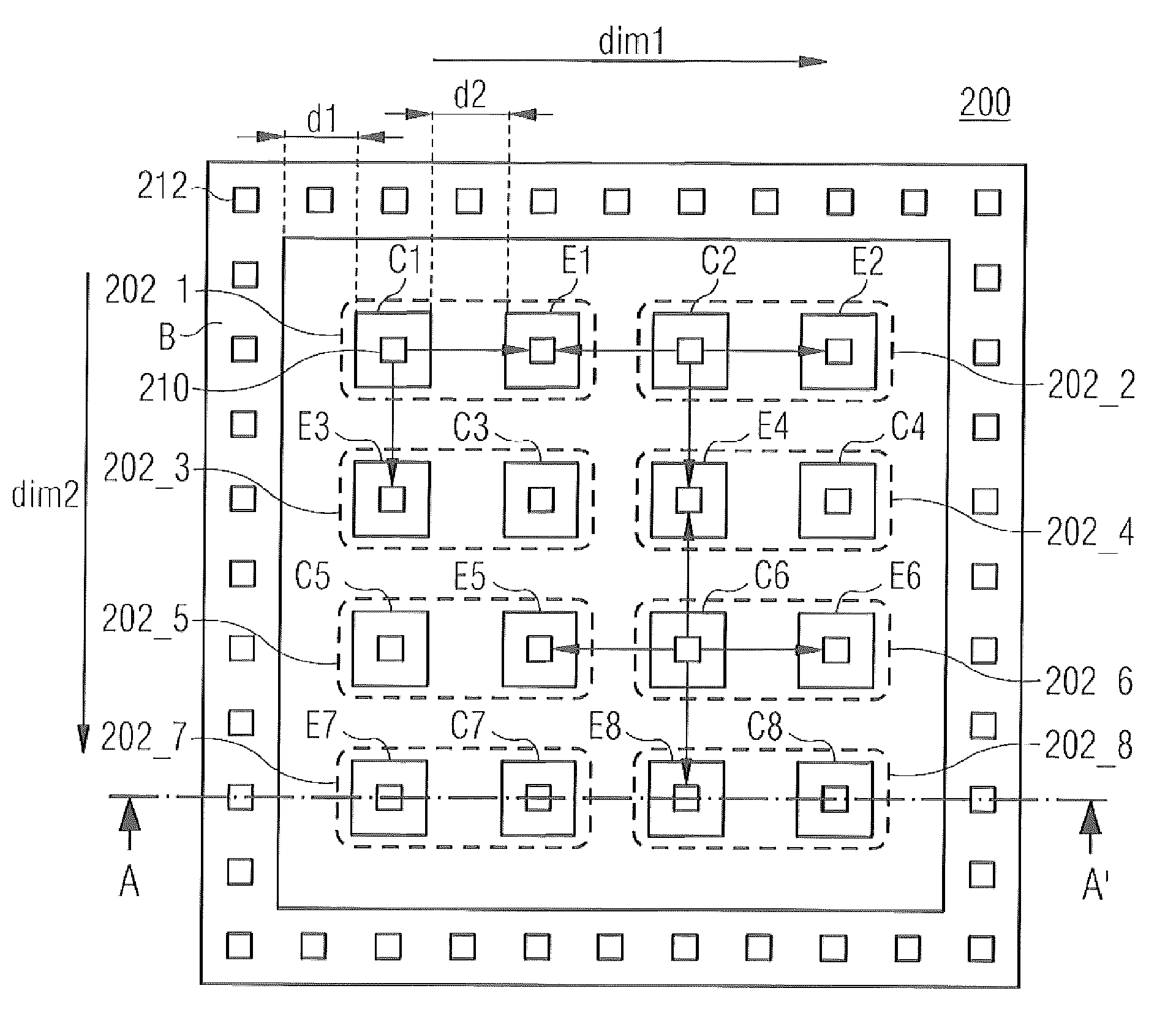
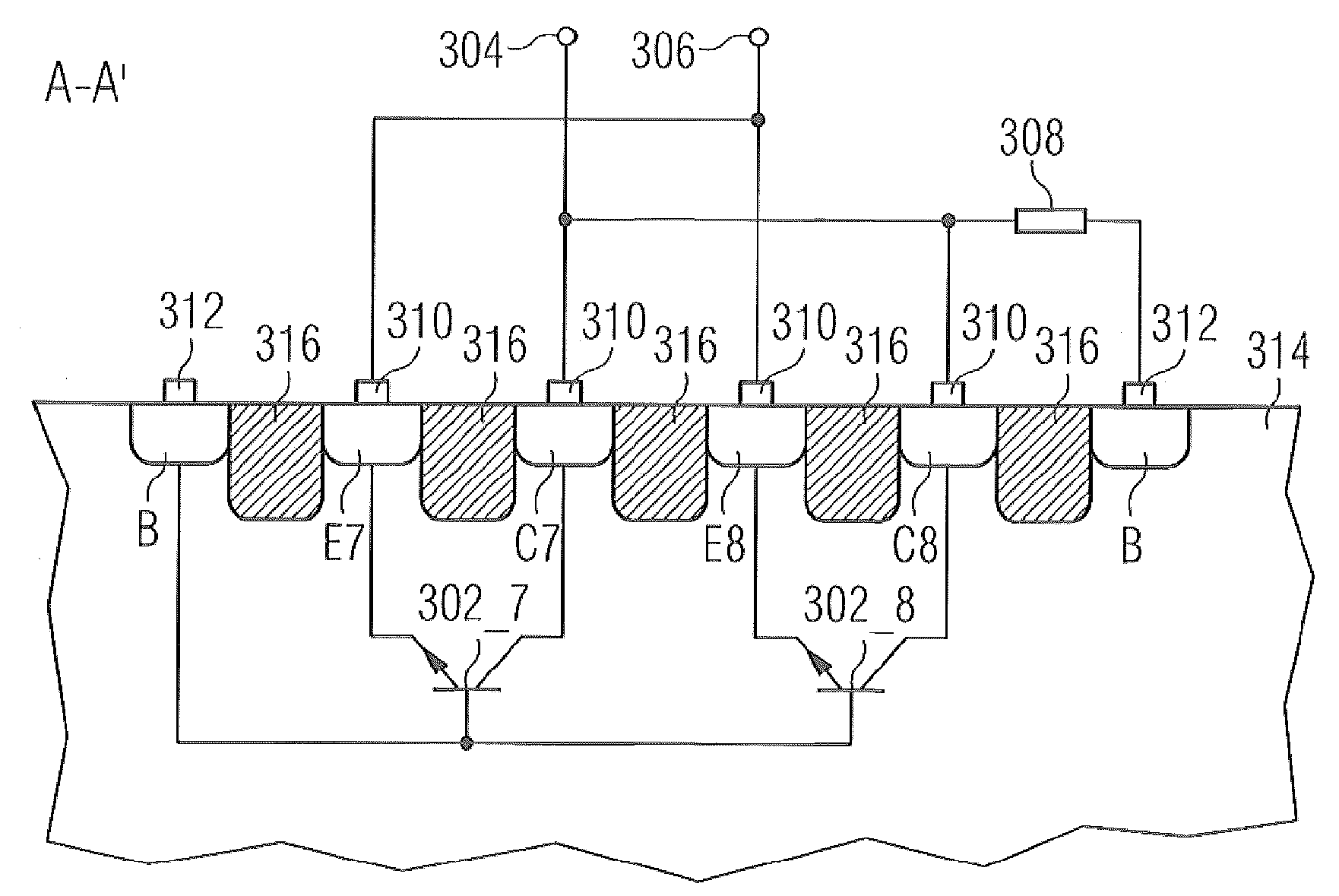
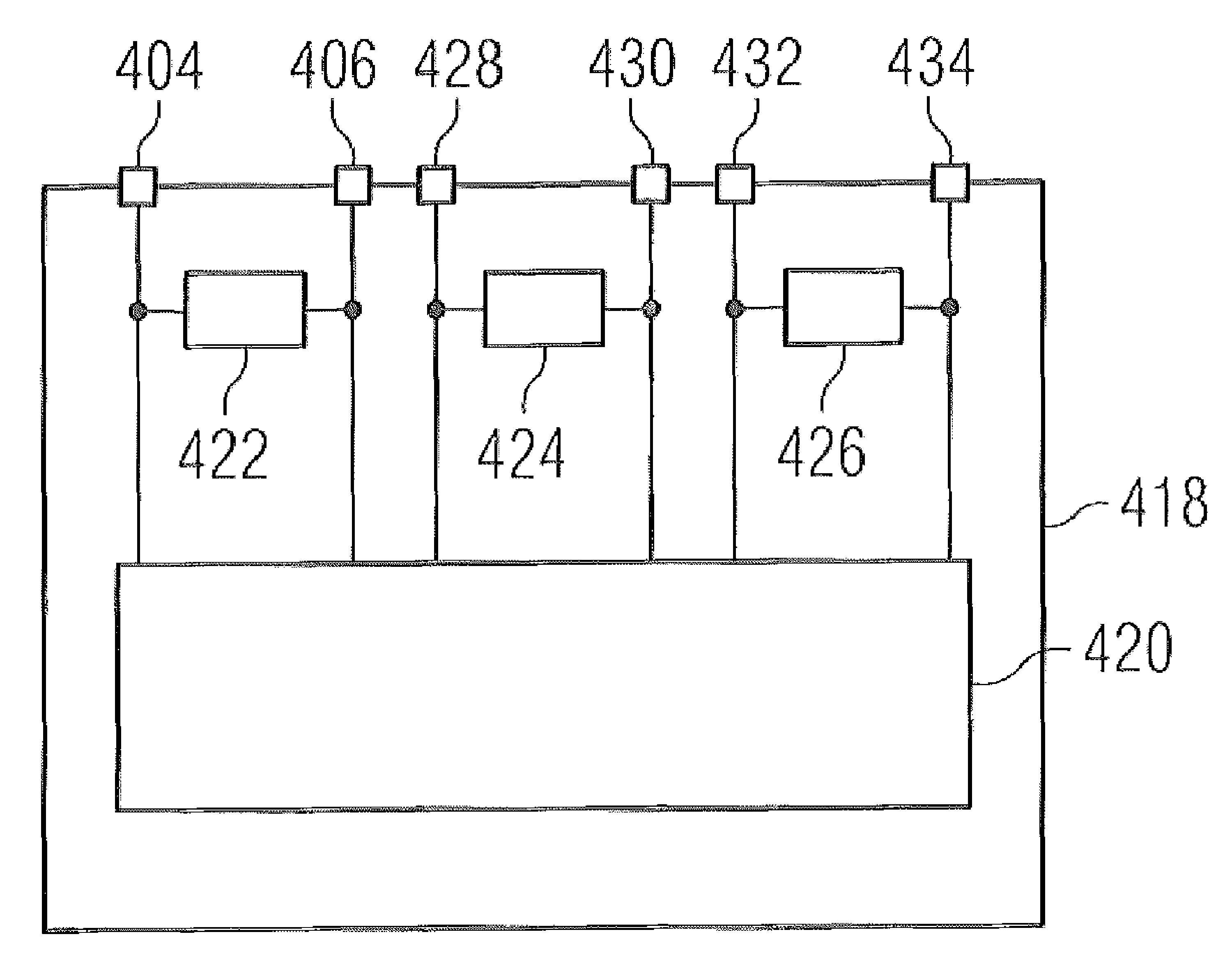
[0013] figure 1 A schematic circuit diagram of an exemplary ESD protection structure 100 comprising a plurality of transistors 102_1 , 102_2 . . . 102_n is shown. The plurality of transistors 102_1 , 102_2 . . . 102_n are all of the same type. together with figure 1 In the illustrated and described embodiment, the plurality of transistors 102_1 , 102_2 . . . 102_n are npn bipolar junction transistors (BJTs). The plurality of npn transistors 102_1 , 102_2 . . . 102_n are coupled in parallel, ie, the collector terminal C1 of the first transistor 102_1 , the collector terminal C2 of the second transistor 102_2 , and the collector terminal Cn of the nth transistor 102_n are coupled to each other. Furthermore, the emitter terminal E1 of the first transistor 102_1 , the emitter terminal E2 of the second transistor 102_2 , and the emitter terminal En of the nth transistor 102_n are coupled to each other. Furthermore, the base terminal B1 of the first transistor 102_1 , the base te...
PUM
 Abstract
Description
Claims
Application Information
 - R&D
- Intellectual Property
- Life Sciences
- Materials
- Tech Scout
- Unparalleled Data Quality
- Higher Quality Content
- 60% Fewer Hallucinations
Browse by: Latest US Patents, China's latest patents, Technical Efficacy Thesaurus, Application Domain, Technology Topic, Popular Technical Reports.
© 2025 PatSnap. All rights reserved.Legal|Privacy policy|Modern Slavery Act Transparency Statement|Sitemap|About US| Contact US: help@patsnap.com


