
A light-emitting component with reflection and current blocking characteristics and a manufacture method thereof

A technology for light-emitting components and manufacturing methods, which is applied in the direction of electrical components, circuits, semiconductor devices, etc., can solve the problems of not considering the loss of external quantum efficiency, increasing equipment costs and production costs, and complicating the process, so as to achieve increased adhesion , high reliability, and the effect of increasing the contact area

Active Publication Date: 2014-06-25
广东昭信集团股份有限公司
View PDF6 Cites 10 Cited by
  • Summary
  • Abstract
  • Description
  • Claims
  • Application Information

AI Technical Summary

Problems solved by technology

Wherein, the light-emitting diode chip is covered by a sealing body, and a metal reflective layer is arranged around the side surface of the sealing body to form a light-transmitting surface on the top surface of the sealing body, thereby reducing light loss and improving the external quantum to a certain extent. efficiency, however it does not take into account the loss of external quantum efficiency due to the absorption of light by the metal electrodes on the top surface
[0004] Chinese patent application 201010200860.1 discloses a gallium nitride-based flip-chip light-emitting diode with an upper reflective layer on the side and its preparation method. Its side has both a Bragg reflective layer and a metal reflective layer, which can improve the external quantum efficiency to a certain extent, but It also does not take into account the loss of external quantum efficiency caused by the absorption of light by metal electrodes located on the light emitting surface
However, the introduction of silicon dioxide greatly increases the equipment cost and production cost, and also makes the process more complicated.

Method used


Image

  • A light-emitting component with reflection and current blocking characteristics and a manufacture method thereof
  • A light-emitting component with reflection and current blocking characteristics and a manufacture method thereof
  • A light-emitting component with reflection and current blocking characteristics and a manufacture method thereof

Examples


Embodiment Construction

[0043] The technical solution of the present invention will be described in detail below in conjunction with the accompanying drawings and specific embodiments.

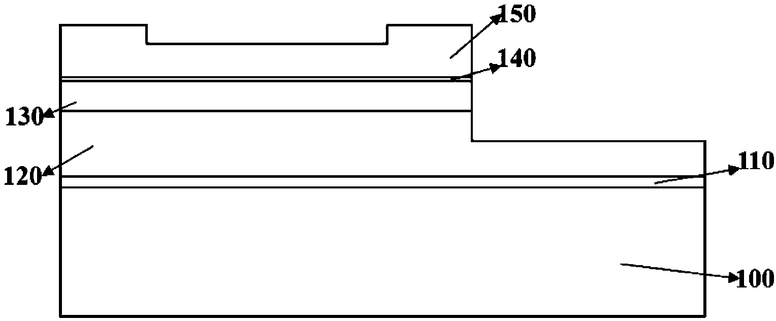
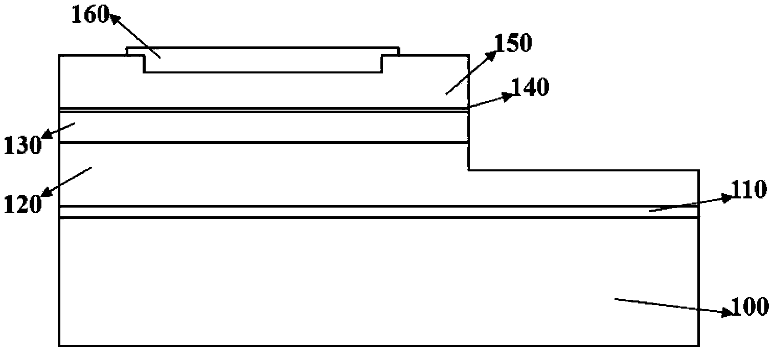
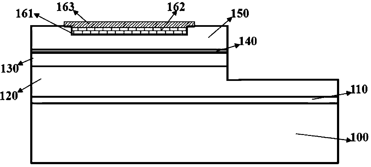
[0044] According to one embodiment of the present invention, there is provided a light emitting element having reflective and current blocking properties. For gallium nitride-based light-emitting devices, in order to reduce the light emitted by the active layer from being absorbed by the pad to the metal electrode, one way is to introduce a metal reflective layer between the metal electrode and the p-type gallium nitride epitaxial layer , such as silver or aluminum reflective layers. However, direct contact between silver and aluminum and the p-type gallium nitride epitaxial layer is not strong, and the phenomenon of electrode detachment is prone to occur, thus hindering the application of metal reflective electrodes. However, this embodiment overcomes the above-mentioned problems.

[0045] The preparation steps of...


PUM


Abstract

The invention provides a light-emitting component with reflection and current blocking characteristics and a manufacture method thereof. The method comprises the following steps 1) growing a buffer layer, an n-type gallium-nitride-based epitaxial layer, an active layer and a p-type gallium-nitride-based layer on a substrate epitaxially in sequence; 2)etching a groove in the surface of the p-type gallium-nitride layer; 3) filling the groove in the p-type gallium-nitride layer with a metallic reflection material; 4) preparing a current blocking layer, wherein the current blocking layer covers the metallic reflection material; and 5) preparing a transparent conductive layer on the current blocking layer, and at last preparing a p-type electrode and an n-type electrode. According to the light-emitting component with the reflection and current blocking characteristics and the manufacture method thereof, external quantum efficiency of the light-emitting component can be improved; the cost is low; process is simple and the reliability is high.

Description

technical field [0001] The invention relates to gallium nitride-based light-emitting element technology, in particular, the invention relates to a light-emitting element with both reflection and current blocking properties and a manufacturing method thereof. Background technique [0002] With the continuous development of human society, energy consumption is increasing, and the global energy shortage has become the consensus of everyone. The semiconductor light-emitting elements have the advantages of high durability, long life, light weight, and low power consumption, making them the focus of governments, colleges and related institutions. Judging from the existing technology, gallium nitride-based light-emitting elements are the basis for realizing semiconductor lighting. With the continuous development and progress of epitaxial growth and chip process technology, its internal quantum efficiency can reach more than 90%. Relatively speaking, the external quantum efficienc...

Claims


Application Information

Patent Timeline
Patent Type & Authority Applications(China)
IPC IPC(8): H01L33/14H01L33/10
CPCH01L33/007H01L33/10H01L33/14
Inventor 李琦
Owner 广东昭信集团股份有限公司
Learn More