Graphene or carbon nanotube devices with localized bottom gates and gate dielectric

一种栅极电介质、碳基纳米的技术,应用在用于材料和表面科学的纳米技术、电固体器件、用于信息加工的纳米技术等方向,能够解决迁移率受损、均匀性损害、输运性质劣化等问题

Active Publication Date: 2014-06-11
INT BUSINESS MASCH CORP
View PDF4 Cites 15 Cited by
  • Summary
  • Abstract
  • Description
  • Claims
  • Application Information

AI Technical Summary

Problems solved by technology

However, molecular layers have been shown to interact with carbon bonds, thereby creating scattering centers that cause substantial impairment of mobility
In fact, since all carriers are located on the surface of these nanostructures, the carriers are strongly coupled to any material deposited around them, causing degradation in transport properties
Furthermore, when molecules such as deoxyribonucleic acid (DNA) are used to create the nucleation layer around carbon nanotubes, uniformity suffers due to the large molecular diameter (4nm for DNA) compared to carbon nanotubes (about 1.5nm). got damage
The latter two methods do not provide a solution for scaling down the dielectric thickness, i.e. dielectric thickness from 8nm to about 15nm is required to ensure complete coverage of the carbon surface

Method used


Image

  • Graphene or carbon nanotube devices with localized bottom gates and gate dielectric
  • Graphene or carbon nanotube devices with localized bottom gates and gate dielectric
  • Graphene or carbon nanotube devices with localized bottom gates and gate dielectric

Examples


Embodiment Construction

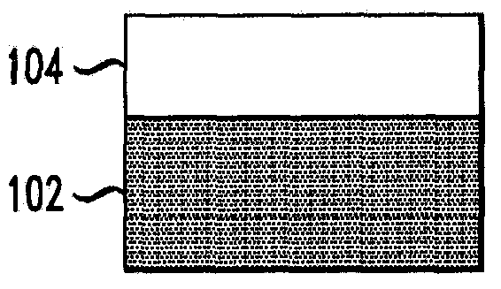
[0035] Provided herein are localized bottom-gate transistor devices and methods for fabricating the devices, wherein the transistor devices have channels formed from nanoscale materials such as carbon nanotubes or graphene, and wherein the bottom-gate dielectric (or at least the lower layer of the multilayer bottom-gate dielectric) is localized to the local gate region. The manufacturing process can be carried out in a variety of different ways.

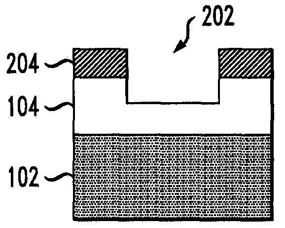
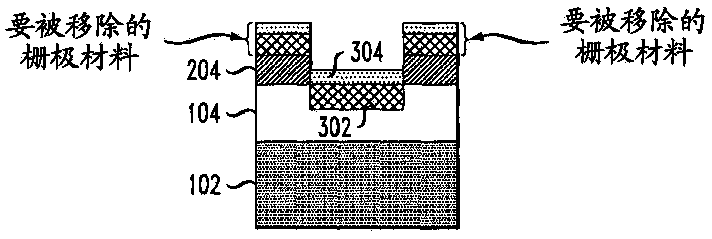
[0036] In a first exemplary embodiment, a gate dielectric local to the bottom gate (or at least a lower layer of a multilayer bottom gate dielectric) is formed on the bottom gate that has been embedded in a trench within an insulator. To ensure a structure where the gate dielectric is localized to the bottom gate (ie, the gate dielectric is precisely aligned with and has the same lateral dimensions as the bottom gate), a self-aligned gate dielectric formation process is utilized. Two self-aligned methods in which the formation of th...


PUM


Abstract

Transistor devices having nanoscale material-based channels (e.g., carbon nanotube or graphene channels) and techniques for the fabrication thereof are provided. In one aspect, a transistor device is provided. The transistor device includes a substrate; an insulator on the substrate; a local bottom gate embedded in the insulator, wherein a top surface of the gate is substantially coplanar with a surface of the insulator; a local gate dielectric on the bottom gate; a carbon-based nanostructure material over at least a portion of the local gate dielectric, wherein a portion of the carbon-based nanostructure material serves as a channel of the device; and conductive source and drain contacts to one or more portions of the carbon-based nanostructure material on opposing sides of the channel that serve as source and drain regions of the device.

Description

[0001] Statement of Government Rights [0002] This invention was made with Government support under Contract No. FA8650-08-C-7838 assigned by the Defense Advanced Research Projects Agency (DARPA). The government has certain rights in this invention. technical field [0003] The present invention relates to transistor devices, and more particularly to transistor devices having channels based on nanoscale materials, such as carbon nanotube or graphene channels, and techniques for fabricating the devices. Background technique [0004] Integrating carbon nanostructures as channel materials in next-generation electronic devices could offer numerous benefits over continued scaling down of silicon (Si). Carbon nanotubes and graphene are two nanoscale forms of carbon that exhibit extremely high current carrying capacity and mobility several orders of magnitude beyond the theoretical limit for Si. Furthermore, carbon nanotubes (one-dimensional) and graphene (two-dimensional) are l...

Claims


Application Information

Patent Timeline
Patent Type & Authority Applications(China)
IPC IPC(8): H03H11/46H01L29/16
CPCH01L51/0023H01L29/1075B82Y30/00H01L29/42384H01L51/055H01L29/78684H01L29/1606H01L29/66742H01L51/0048H01L29/7781B82Y10/00H01L51/0545H01L29/4908H10K71/621H10K85/221H10K10/481H10K10/466
Inventor 陈志宏A·D·富兰克林汉述仁J·B·汉拿恩K·L·萨恩格G·S·土利维斯盖
Owner INT BUSINESS MASCH CORP
Why Eureka
Try Eureka