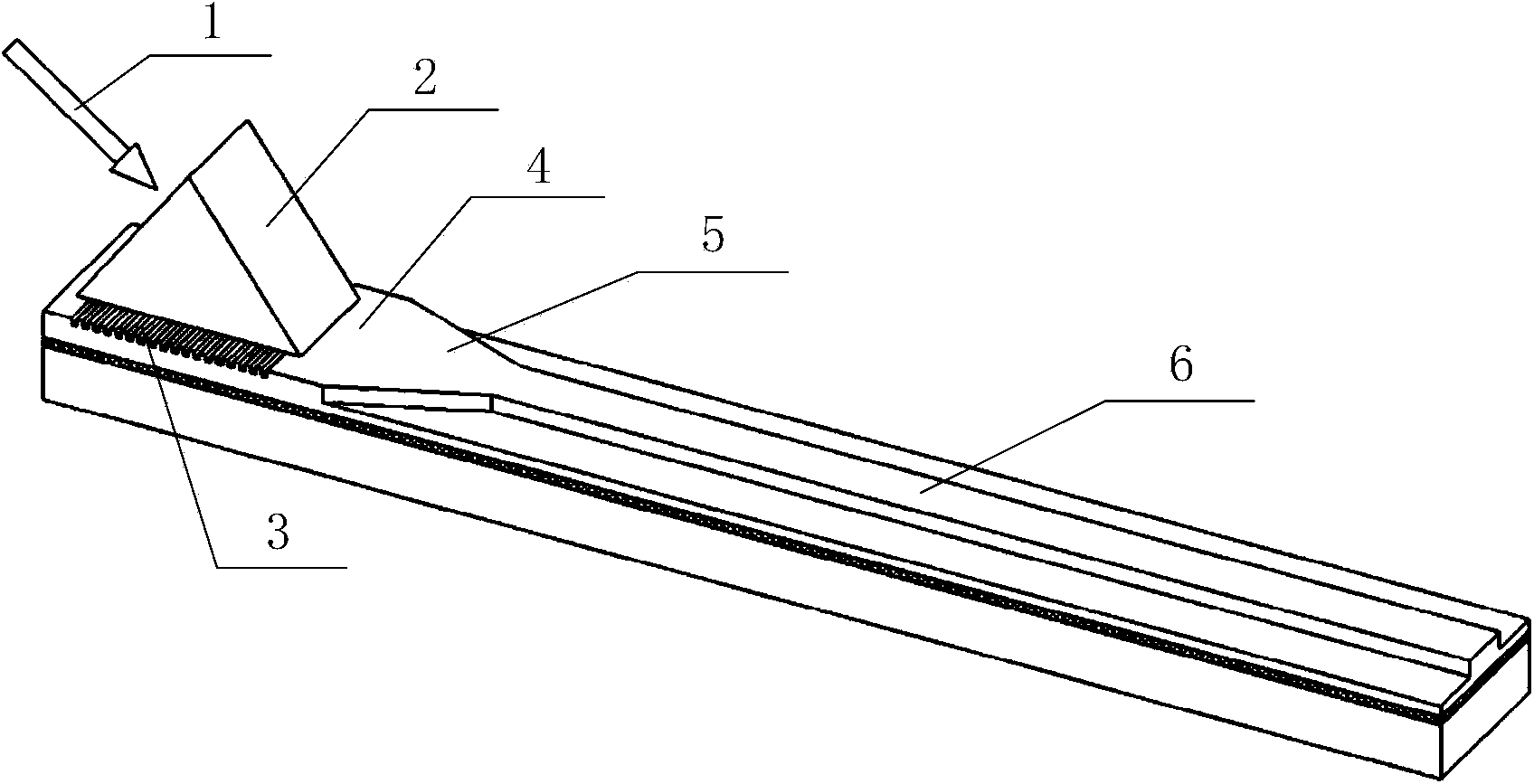
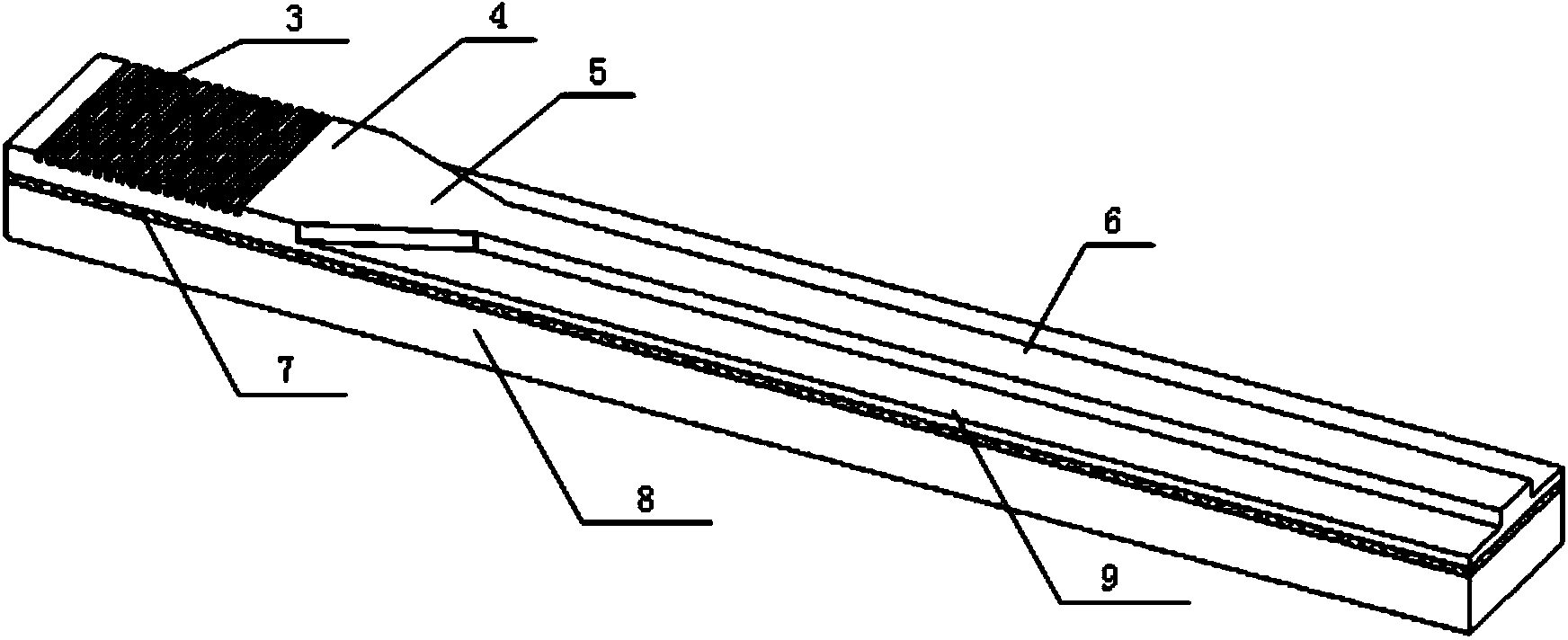
Prism-grating optical waveguide coupler and optical waveguide device
A technology of optical waveguide coupling and optical waveguide, which is applied in the field of optical waveguide, can solve the problems of inapplicability of prism coupler, difficult realization of grating manufacturing technology, and short grating period.
- Summary
- Abstract
- Description
- Claims
- Application Information
AI Technical Summary
Problems solved by technology
Method used
Image
Examples
example 1
[0055] The schematic diagram of the material structure of SOI ridge optical waveguide is shown in Figure 5 As shown, the intermediate insulating layer made on the silicon substrate is SiO 2 Layer 8, SiO 2 Layer 8 has a refractive index of 1.462 and a thickness of 0.2 μm. The silicon top layer is fabricated on the insulating layer, and the refractive index of Si is 3.476. The outer ridge height h=5.5 μm of the ridge waveguide, the inner ridge height H=8.5 μm, the width of the optical waveguide is 10 μm, and the ridge width is 4 μm. The thickness of the silicon top layer of the planar waveguide is H=8.5μm, and the width of the optical waveguide is 10μm.
[0056] The wavelength of incident light in vacuum is set as λ=1550nm. Using the BeamProP module in the Rsoft software to simulate the planar waveguide, the effective refractive index of the 0th-order guided mode is n eff =3.4742. Choose the material refractive index of the prism n p = 2.1, then there is Only the first...
PUM
 Abstract
Description
Claims
Application Information
 - R&D
- Intellectual Property
- Life Sciences
- Materials
- Tech Scout
- Unparalleled Data Quality
- Higher Quality Content
- 60% Fewer Hallucinations
Browse by: Latest US Patents, China's latest patents, Technical Efficacy Thesaurus, Application Domain, Technology Topic, Popular Technical Reports.
© 2025 PatSnap. All rights reserved.Legal|Privacy policy|Modern Slavery Act Transparency Statement|Sitemap|About US| Contact US: help@patsnap.com


