A kind of back contact crystalline silicon cell and its manufacturing method

A technology of crystalline silicon battery and manufacturing method, which is applied in the field of solar cells, can solve the problems of increasing the difficulty and complexity of the manufacturing process, affecting the mechanical strength of the device, and increasing the production cost, so as to avoid shading loss and improve electrical performance and reliability , the effect of reducing production costs

Active Publication Date: 2017-01-25
紫石能源有限公司
View PDF3 Cites 0 Cited by
  • Summary
  • Abstract
  • Description
  • Claims
  • Application Information

AI Technical Summary

Problems solved by technology

[0005] Although this technology avoids the shading loss caused by the electrodes on the light-receiving surface, in order to ensure that the current on the light-receiving surface is transmitted to the non-light-receiving surface without loss, tens of thousands of openings need to be made on the crystalline silicon wafer, and a high concentration of Doped PN junction, the manufacturing process is very complicated, and increases the production cost; at the same time, too many openings also affect the mechanical strength of the device, which will lead to a large number of silicon chips being broken during production
In addition, in the process of making electrodes, it is necessary to keep a necessary gap between the end of the electrode sub-grid and the main grid, which also increases the difficulty and complexity of the manufacturing process.

Method used


Image

  • A kind of back contact crystalline silicon cell and its manufacturing method
  • A kind of back contact crystalline silicon cell and its manufacturing method
  • A kind of back contact crystalline silicon cell and its manufacturing method

Examples


Embodiment 1

[0037] The specific production method steps include:

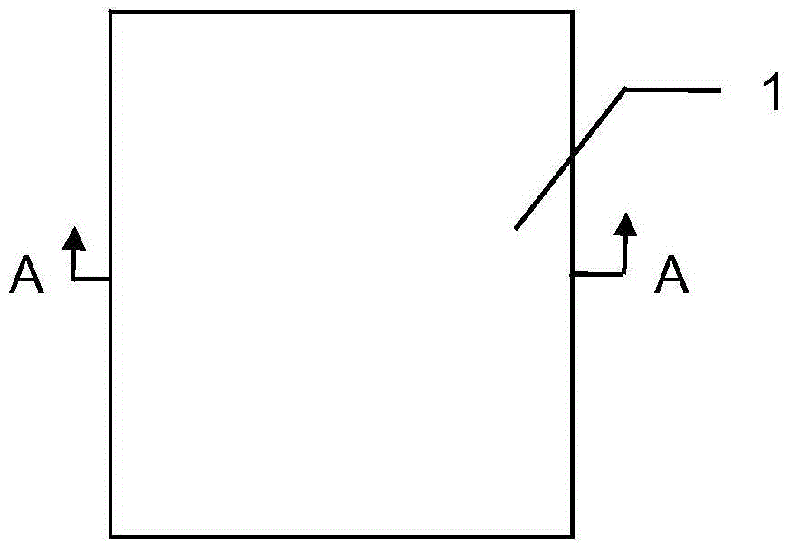
[0038] Step 1: If figure 1 As shown, the surface of the silicon wafer is pretreated to remove surface impurities and surface oxide layers, and after completion, it is cleaned with deionized water.

[0039] Step 2: Anisotropic texture is chemically etched on the surface of the N-type silicon substrate 1 to produce a pyramid-shaped light-trapping structure.

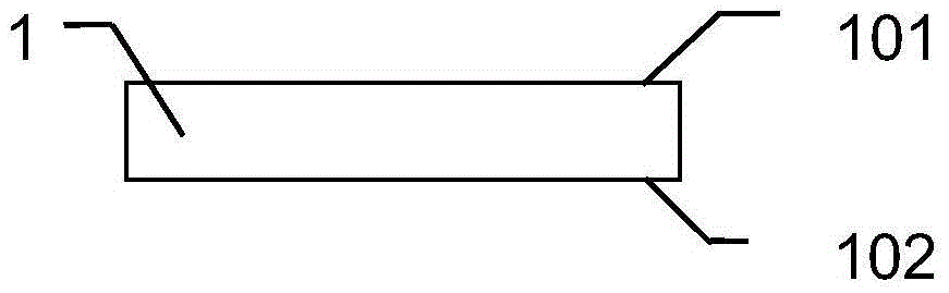
[0040] Step 3: If figure 2 1. Perform a polishing process on the non-light-receiving surface 101 of the silicon substrate 1 forming the textured structure, and perform standard cleaning on the silicon wafer after polishing. The cleaning process is the same as step 1.

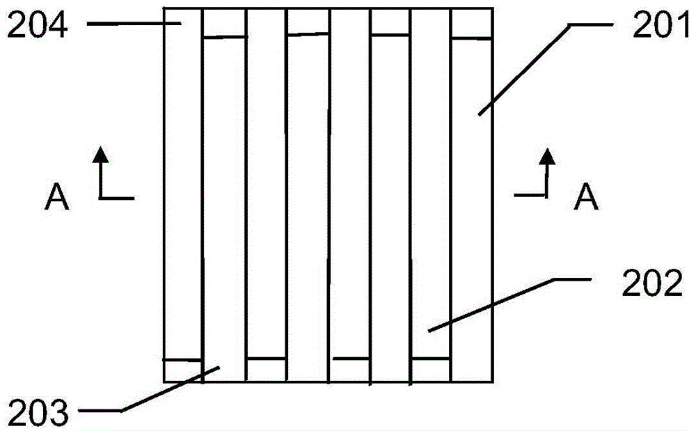
[0041] Step 4: If Figures 3 to 4As shown, the method of ion implantation is used to do boron (B) doping on the non-light-receiving surface 101 of the silicon substrate, the energy of ion implantation is 1-200keV, and the dose is 5x10 14 ~5x10 17 / cm 2 , the time is 1-60s, and the substrate tempera...

Embodiment 2

[0053] Optimized with respect to Example 1.

[0054] Step 9: Using sputtering, thermal evaporation or electroplating metallization process, fabricate a P-type area converging conductive belt 301 above the P-type area 201 of the solar cell, and fabricate an N-type area converging conductive belt 302 above the N-type area 202 of the non-light-receiving surface of the battery .

Embodiment 3

[0056] Optimized with respect to Example 1.

[0057] Step 9: Using sputtering, thermal evaporation or electroplating metallization process, fabricate a P-type area converging conductive belt 301 above the P-type area 201 of the solar cell, and fabricate an N-type area converging conductive belt 302 above the N-type area 202 of the non-light-receiving surface of the battery . The P-type region converging conductive strip 301 and the N-type region converging conductive strip 302 are Al, Ag, Au, Ni, Cu, Cu / Ni, Al / Ni or Ti / Pd / Ag electrodes, and their thickness is 0.05um-600um , and the P-type area busbars 301 and the N-type area busbars 302 are alternately arranged, that is, an arrangement structure of P-N-P-N area busbars is formed.


PUM

PropertyMeasurementUnit
thicknessaaaaaaaaaa
thicknessaaaaaaaaaa

Abstract

The invention provides a back-contact crystalline silicon cell which comprises a silicon substrate (1). The silicon substrate (1) comprises a silicon substrate non-illuminated face (101). The back-contact crystalline silicon cell also comprises a PN-doped area (2) positioned on the silicon substrate non-illuminated face (101). The PN-doped area (2) contains alternately-arranged P-type areas (201) and N-type areas (202) having convergence conductive bands on the surface thereof, wherein along the extension direction of each P-type area (201) or N-type area (202), there is distance difference between adjacent strips; a first strip between adjacent strips is along the extension direction; a part over a second strip is taken as an edge strip of the first strip; the edge strip is a P-type area edge strip (203) or N-type area edge strip (204); and the edge strip is taken as an electrode lead-out part. The invention also provides a manufacturing method of the back-contact crystalline silicon cell. According to the manufacturing method, a trepanning step and a step of keeping a necessary gap between an electrode auxiliary grid end and a main grid are avoided, manufacturing process is simplified, and production cost is reduced.

Description

technical field [0001] The invention belongs to the field of solar cells, in particular to a back contact crystalline silicon cell and a manufacturing method thereof. Background technique [0002] In today's national economic development process, fossil energy plays an important role as the main source of energy. However, as a traditional non-renewable energy source, fossil energy is increasingly depleted. Among the existing sustainable energy sources, solar energy has many advantages such as cleanness, safe use, inexhaustibility, low utilization cost, and no geographical restrictions. It is one of the ideal energy sources to solve energy and environmental problems, and has broad development prospects. . [0003] Although photovoltaic technology has developed by leaps and bounds in recent years, how to further improve battery efficiency and reduce costs is still an urgent problem to be solved. The technical solution adopted by metal wrapthrough (MWT, metal wrapthrough) sol...

Claims


Application Information

Patent Timeline
Patent Type & Authority Patents(China)
IPC IPC(8): H01L31/0224H01L31/068H01L31/18
CPCH01L31/02167H01L31/022441H01L31/0682H01L31/1804H01L31/1868Y02E10/547Y02P70/50
Inventor 李鸿儒兰立广童翔
Owner 紫石能源有限公司
Why Eureka
Try Eureka