Melting process for polycrystalline silicon cast ingots
A technology of polysilicon and melting material, which is applied in the direction of polycrystalline material growth, crystal growth, single crystal growth, etc., can solve the problems of insufficient melting time, too long melting time, and the decline in the quality of polysilicon ingots, etc., to achieve convenient, The effect of reducing the sticking rate and improving the quality of crystal growth
- Summary
- Abstract
- Description
- Claims
- Application Information
AI Technical Summary
Problems solved by technology
Method used
Image
Examples
Embodiment 1
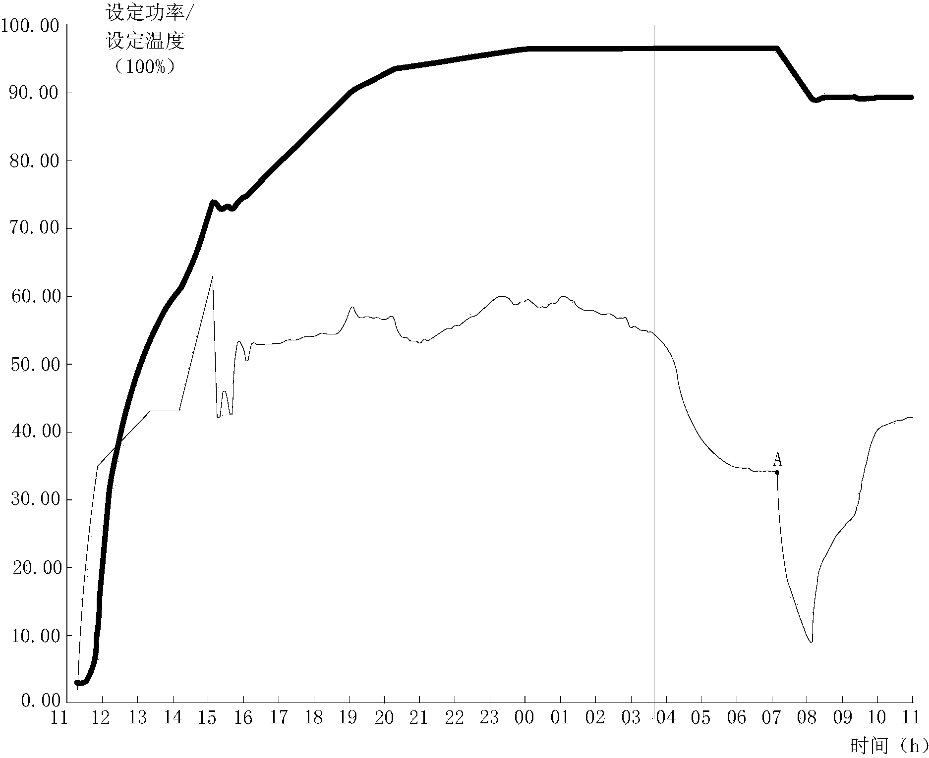
[0036] Such as figure 1 The shown melt process for polycrystalline silicon ingots includes the following steps:
[0037] Step 1. Preheating: Preheat the silicon material contained in the crucible with an ingot furnace, and gradually increase the heating temperature of the ingot furnace to T1; the preheating time is 7h, where T1=1175°C.
[0038] In this embodiment, the ingot furnace is a G5 ingot furnace. Moreover, the ingot furnace is specifically a G5 ingot furnace produced by Zhejiang Jingsheng Electromechanical Co., Ltd. The crucible is a quartz crucible and it is a G5 crucible, and the produced polysilicon ingot is a G5 ingot.
[0039] In actual use, the charging amount of the quartz crucible is about 600 kg.
[0040] In this embodiment, the charging amount of the quartz crucible is 560 kg. During actual use, the charging amount of the quartz crucible can be adjusted accordingly according to specific needs.
[0041] In this embodiment, during the preheating process in step 1, the...
Embodiment 2
[0074] In this embodiment, the difference from embodiment 1 is: the preheating time in step 1 is 6h and T1=1185°C, P1=80kW; in step 2, T5=1560°C, t=18min, Q1=650mbar; step 1. The medium holding time is 0.4h; from step 2 to step 5, T2=1210℃, and the heating time is 0.4h; in step 6 T3=1460℃ and the heating time is 3.5h; in step 7, T4=1510℃ and The heating time is 3.5h; in the 8th step, T5=1560℃ and the heating time is 3.5h; the 9th step is 3.5h; the 10th step is 4h.
[0075] In this embodiment, the process of heating and pressurizing in steps 2 to 5 is as follows:
[0076] The second step, the first step is to increase: the heating temperature of the ingot furnace is increased from 1185°C to 1190°C, and the heating time is 5 min.
[0077] Step 3 and Step 2: Increase the heating temperature of the ingot furnace from 1190°C to 1195°C, and the heating time is 5 minutes.
[0078] Step 4 and Step 3: Raise the heating temperature of the ingot furnace from 1195°C to 1205°C, and the heating ti...
Embodiment 3
[0083] In this embodiment, the difference from embodiment 1 is: the preheating time in step one is 10h and T1=1165°C, P1=70kW; in step two, T5=1540°C, t=22min, Q1=550mbar; step 1. The medium holding time is 0.6h; from step 2 to step 5, T2=1190℃ and the heating time is 0.6h; in step 6 T3=1440℃ and the heating time is 4.5h; in step 7 T4=1490℃ and The heating time is 4.5h; in the 8th step, T5=1540℃ and the heating time is 4.5h; the 9th step is 4.5h; the 10th step is 8h.
[0084] In this embodiment, the process of heating and pressurizing in steps 2 to 5 is as follows:
[0085] The second step, the first step is to increase: increase the heating temperature of the ingot furnace from 1165°C to 1172°C, and the heating time is 9 minutes.
[0086] Step 3 and Step 2: Increase the heating temperature of the ingot furnace from 1172°C to 1178°C, and the heating time is 8 minutes.
[0087] Step 4 and Step 3: Increase the heating temperature of the ingot furnace from 1178°C to 1183°C, and the heat...
PUM
 Abstract
Description
Claims
Application Information
 - Generate Ideas
- Intellectual Property
- Life Sciences
- Materials
- Tech Scout
- Unparalleled Data Quality
- Higher Quality Content
- 60% Fewer Hallucinations
Browse by: Latest US Patents, China's latest patents, Technical Efficacy Thesaurus, Application Domain, Technology Topic, Popular Technical Reports.
© 2025 PatSnap. All rights reserved.Legal|Privacy policy|Modern Slavery Act Transparency Statement|Sitemap|About US| Contact US: help@patsnap.com


