Liquid crystal display device and corresponding manufacturing method

A technology of a liquid crystal display device and a manufacturing method, which is applied in nonlinear optics, instruments, optics, etc., can solve the problems of reducing light transmittance, affecting display effect and brightness, etc., so as to avoid poor alignment and improve large-view angle deviation , Improve the effect of transmittance

Inactive Publication Date: 2014-04-16
TCL CHINA STAR OPTOELECTRONICS TECH CO LTD
View PDF9 Cites 11 Cited by
  • Summary
  • Abstract
  • Description
  • Claims
  • Application Information

AI Technical Summary

Problems solved by technology

[0004] But the existing method strongly depends on the electrode design, which will produce obvious bright and dark stripes in the display area, which will reduce the light transmittance, thus affecting the display effect and brightness

Method used


Image

  • Liquid crystal display device and corresponding manufacturing method
  • Liquid crystal display device and corresponding manufacturing method
  • Liquid crystal display device and corresponding manufacturing method

Examples


Embodiment Construction

[0048] The following descriptions of the various embodiments refer to the accompanying drawings to illustrate specific embodiments in which the present invention can be implemented. The directional terms mentioned in the present invention, such as "up", "down", "front", "back", "left", "right", "inside", "outside", "side", etc., are for reference only The orientation of the attached schema. Therefore, the directional terms used are used to illustrate and understand the present invention, but not to limit the present invention.

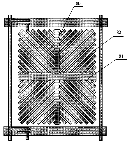
[0049] Such as image 3 and Figure 4 As shown, it is a schematic structural diagram of an embodiment of a liquid crystal display device provided by the present invention, and the liquid crystal display device includes:

[0050] The TFT array substrate 1 has a first electrode layer 15 and a first alignment layer 19 covering the first electrode layer 15, a color filter layer 18 is formed between the glass substrate 11 and the passivation layer 180 of...


PUM


Abstract

The invention discloses a liquid crystal display device. The liquid crystal display device comprises a TFT array substrate, and further comprises a back matrix, photo spacers, a CF substrate and a liquid crystal layer, wherein the TFT array substrate is provided with a first electrode layer and a first alignment layer covering the first electrode layer, a colorful film layer is formed between a glass substrate and a passivation layer of the TFT array substrate, the CF substrate is provided with a second electrode layer and a second alignment layer covering the second electrode layer, the liquid crystal layer is arranged between the first alignment layer of the TFT array substrate and the second alignment layer of the CF substrate, the preset alignment directions of the corresponding alignment areas of the first alignment layer and the second alignment layer are perpendicular to each other, and alignment films corresponding to the preset alignment directions of the alignment areas are formed on the first alignment layer and the second alignment layer. The invention further discloses a manufacturing method of the liquid crystal display device. According to the liquid crystal display device and the manufacturing method of the liquid crystal display device, the alignment effect is good, meanwhile, the large-visual-angle color cast can be improved, and the aperture opening ratio is improved.

Description

technical field [0001] The present invention relates to the field of manufacturing a thin film transistor liquid crystal display (Thin Film Transistor liquid crystal display, TFT-LCD), in particular to a liquid crystal display device and a corresponding manufacturing method. Background technique [0002] Such as figure 1 Shown is a schematic diagram of a pixel electrode commonly used in an existing PSVA mode (Polymer Stabilization Vertical-Alignment) liquid crystal display device; a pixel electrode is shown in the figure. In the existing liquid crystal display device of this PSVA mode, its pixel electrode is designed as a "meter" shape, consisting of a vertical trunk 80 in the middle, a horizontal trunk 81 and an included angle of ±45 degrees with the x-axis, ±135 Branch 82 of the degree consists of three parts. Among them, the vertical trunk 80 and the horizontal trunk 81 divide the pixel area into 4 areas on average, and each area is composed of 45-degree inclined branch...

Claims


Application Information

Patent Timeline
Patent Type & Authority Applications(China)
IPC IPC(8): G02F1/1337G02F1/1335G02F1/136G02F1/1333
CPCG02F1/13394G02F1/133753G02F1/133788G02F1/136209G02F1/133757G02F1/136222G02F1/133514G02F1/1339G02F1/136286G02F1/1368G02F1/1337
Inventor 赵勇张鑫连水池
Owner TCL CHINA STAR OPTOELECTRONICS TECH CO LTD
Why Eureka
Try Eureka