


Quick Research
Generate reliable direction feasibility study reports for your R&D in just a few steps.

Technical Q&A
Discover and master advanced knowledge NOW. Basics, ideas, possibilities, all at once.

Find Solutions
As an expert in R&D theories, this can generate solutions to your technical problems instantly.

Evaluate Feasibility
Analyze your overall solution with one click, know your potential R&D risks in advance.

Monitor Landscape
Get weekly tech updates, stay abreast of the latest tech innovations and key insights.
How the transistor is formed
A technology of transistors and semiconductors, applied in the direction of semiconductor devices, semiconductor/solid-state device manufacturing, electrical components, etc., can solve problems such as poor performance of transistors, and achieve the effect of preventing leakage current, preventing leakage current, and avoiding threshold voltage
- Summary
- Abstract
- Description
- Claims
- Application Information
AI Technical Summary
Problems solved by technology
Method used
Image

Examples
no. 1 example
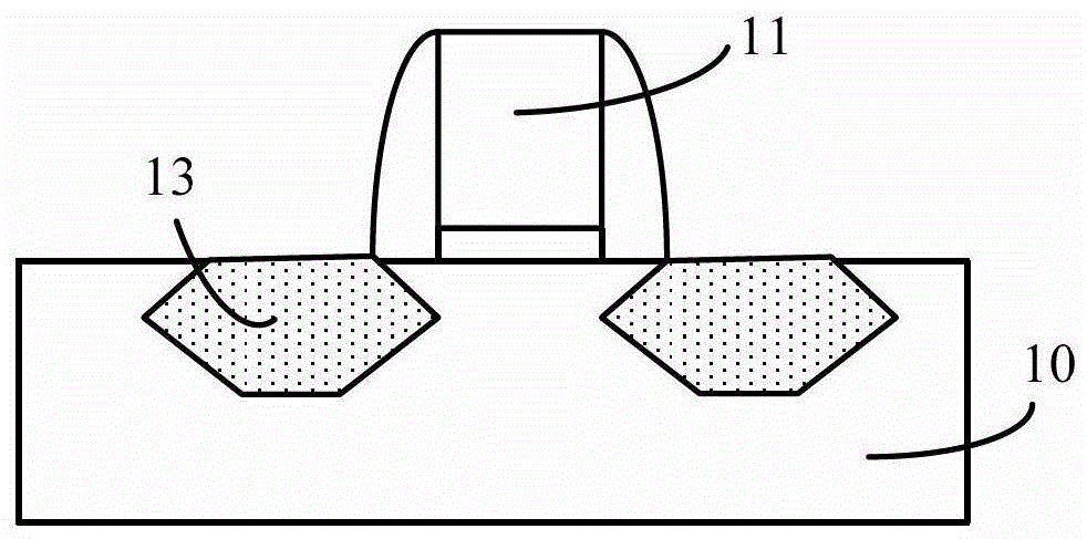
[0044] Figure 5 to Figure 9 It is a schematic cross-sectional structure diagram of the transistor formation process described in the first embodiment of the present invention, including:
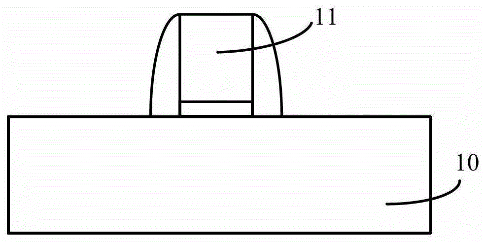
[0045] Please refer to Figure 5 , providing a semiconductor substrate 200 with a gate structure 201 on the surface of the semiconductor substrate 200 .
[0046] The semiconductor substrate 200 is used to provide a working platform for subsequent processes, and the material of the semiconductor substrate 200 is single crystal silicon, or the semiconductor substrate 200 is a silicon-on-insulator (SOI) structure; in this embodiment, Since it is necessary to subsequently form a “Σ”-shaped opening with sidewalls and the surface of the semiconductor substrate 200 in the semiconductor substrate 200 , the crystal plane index of the surface of the semiconductor substrate 200 is (100).
[0047] The gate structure 201 includes: a gate dielectric layer 210 located on the surface of the semiconductor...
no. 2 example
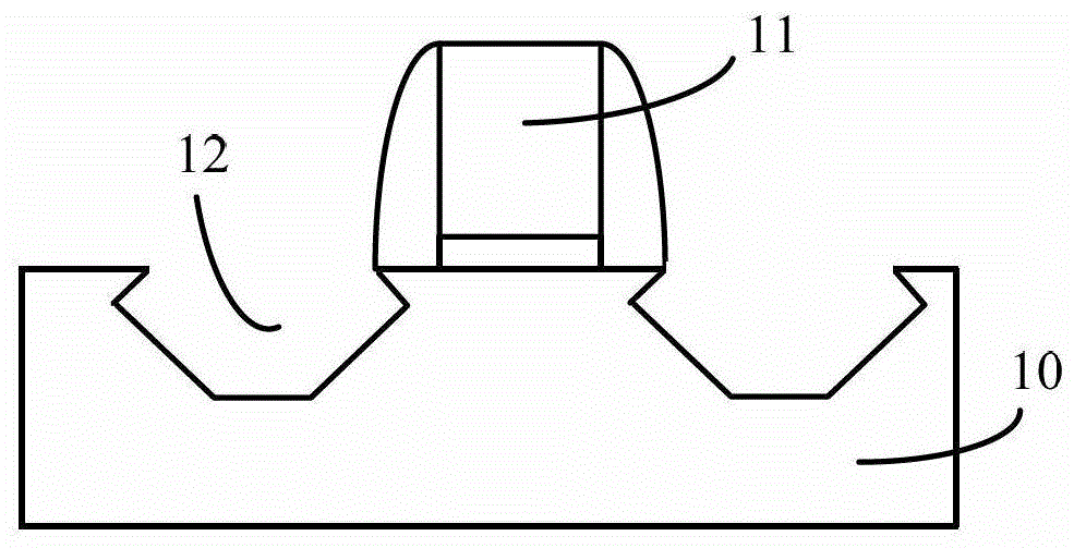
[0075] Figure 10 to Figure 13 It is a schematic cross-sectional structure diagram of the transistor formation process described in the second embodiment of the present invention, including:
[0076] Please refer to Figure 10 , providing a semiconductor substrate 300, the surface of the semiconductor substrate 300 has a gate structure 301; using the gate structure 301 as a mask, forming openings 302 in the semiconductor substrate 300 on both sides of the gate structure 301.
[0077] The semiconductor substrate 300 is used to provide a working platform for subsequent processes, and the material of the semiconductor substrate 300 is single crystal silicon, or the semiconductor substrate 300 is a silicon-on-insulator (SOI) structure; in this embodiment, Since it is necessary to form a “Σ”-shaped opening with sidewalls and the surface of the semiconductor substrate 300 in the semiconductor substrate 300 later, the crystal plane index of the surface of the semiconductor substrate...
PUM
 Abstract
Description
Claims
Application Information
 - R&D Engineer
- R&D Manager
- IP Professional
- Industry Leading Data Capabilities
- Powerful AI technology
- Patent DNA Extraction
Browse by: Latest US Patents, China's latest patents, Technical Efficacy Thesaurus, Application Domain, Technology Topic, Popular Technical Reports.
© 2024 PatSnap. All rights reserved.Legal|Privacy policy|Modern Slavery Act Transparency Statement|Sitemap|About US| Contact US: help@patsnap.com