
Light-emitting component and method for producing a light-emitting component

A light-emitting device and luminescence technology, which is applied in semiconductor/solid-state device manufacturing, semiconductor devices, electric solid-state devices, etc., can solve the problems of research and development costs, achieve high efficiency and service life, and change the effect of color distortion

Inactive Publication Date: 2014-03-19
OSRAM OLED
View PDF5 Cites 1 Cited by
  • Summary
  • Abstract
  • Description
  • Claims
  • Application Information

AI Technical Summary

Problems solved by technology

However, this has hitherto only been possible with relatively high development expenditure due to the multiple cross-correlations of the optical and electrical properties

Method used


Image

  • Light-emitting component and method for producing a light-emitting component
  • Light-emitting component and method for producing a light-emitting component
  • Light-emitting component and method for producing a light-emitting component

Examples


Embodiment Construction

[0045] In the following detailed description, reference is made to the accompanying drawings, which form a part of the description, and in which specific implementation forms that can implement the present invention are shown for illustration. In this regard, directional terms such as "upper", "lower", "front", "rear", "front", "rear", etc. apply in relation to the orientation of the described drawings. Because the components of the implementation form can be positioned in a number of different orientations, the directional terminology is used for illustration and is not limited in any way. It should be understood that other implementation forms can be used and structural or logical changes can be made without departing from the protection scope of the present invention. It goes without saying that, unless otherwise specified, the features of the different exemplary embodiments described herein can be combined with each other. Therefore, the following detailed description shou...


PUM


Abstract

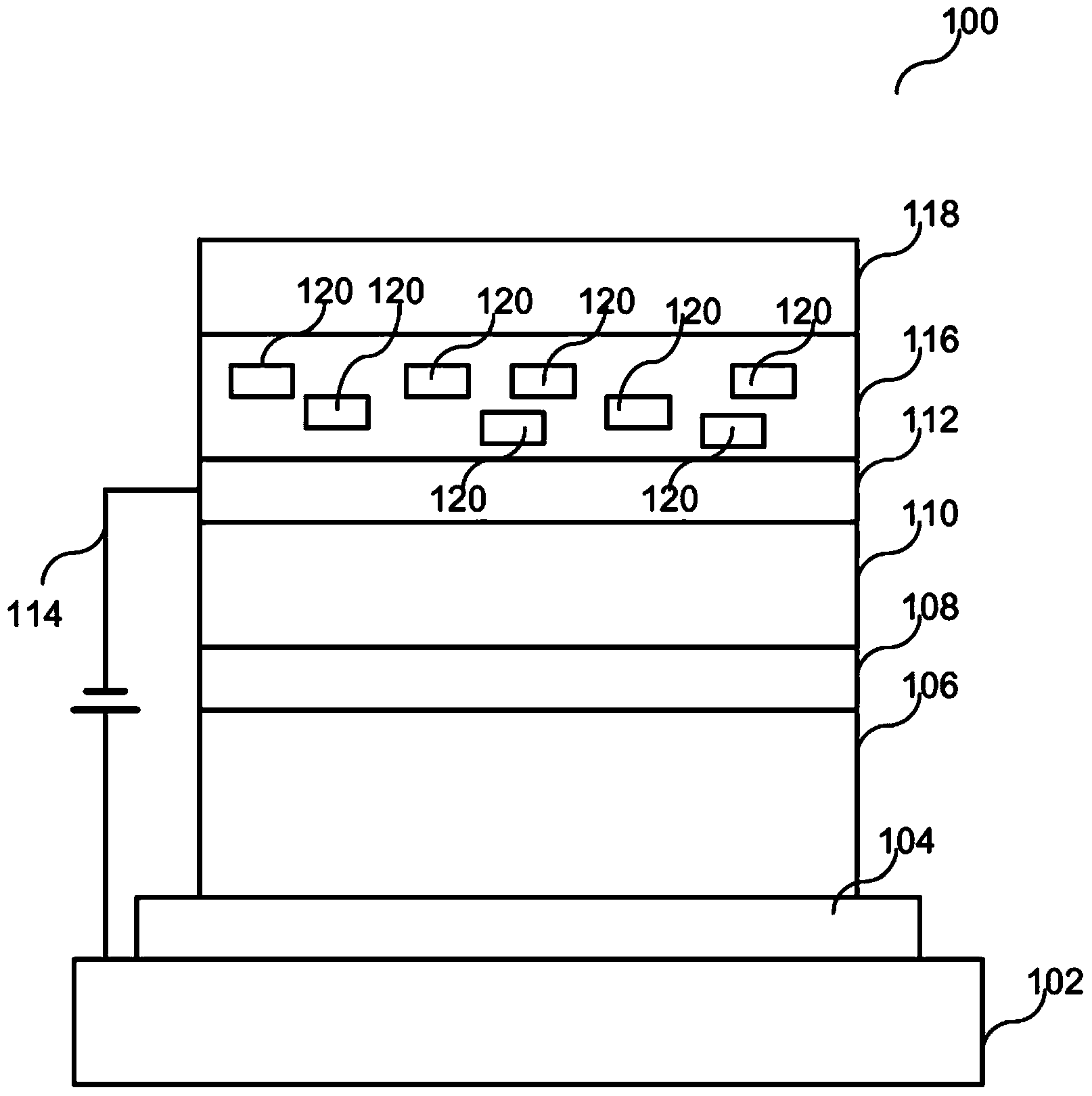
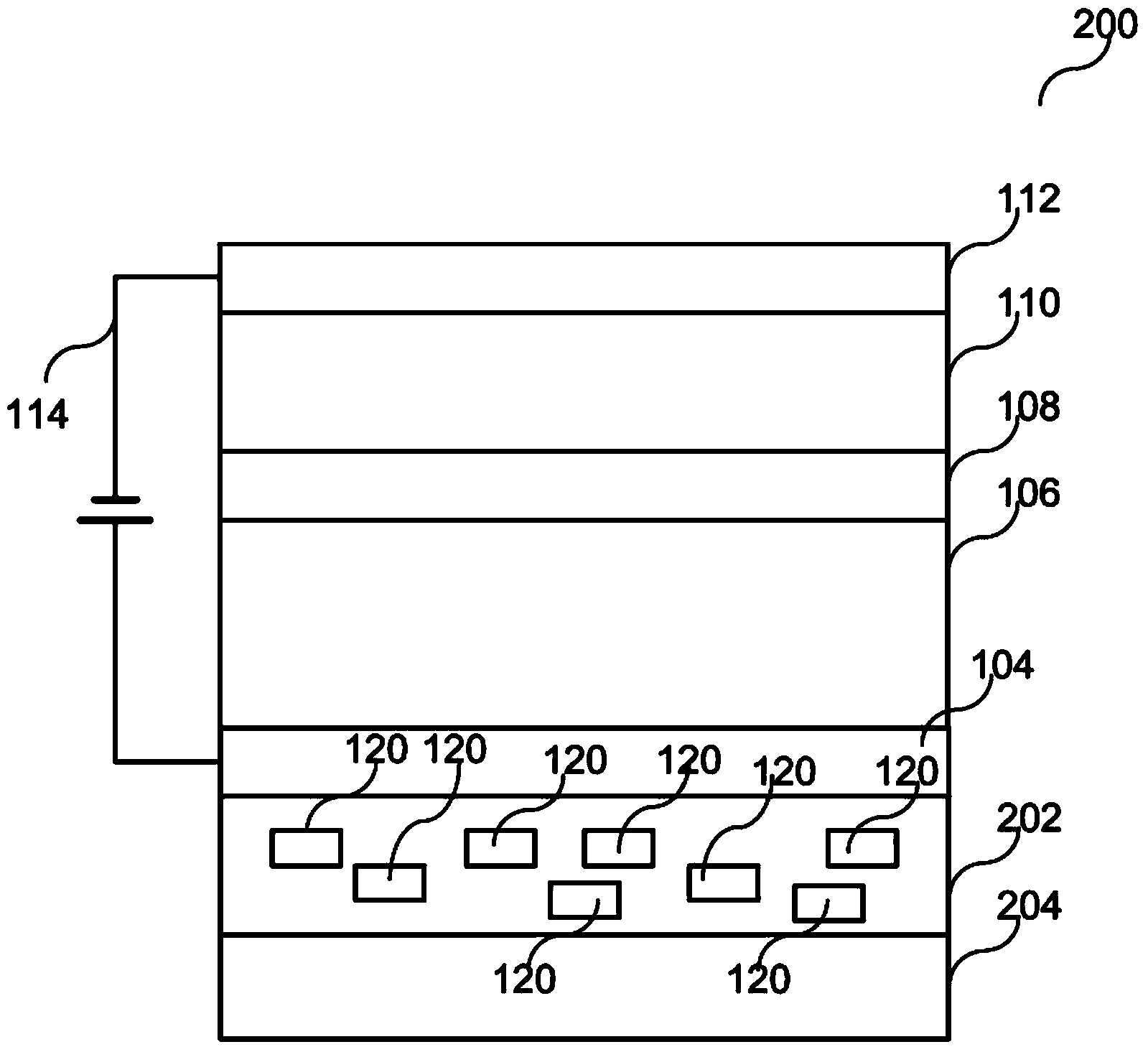
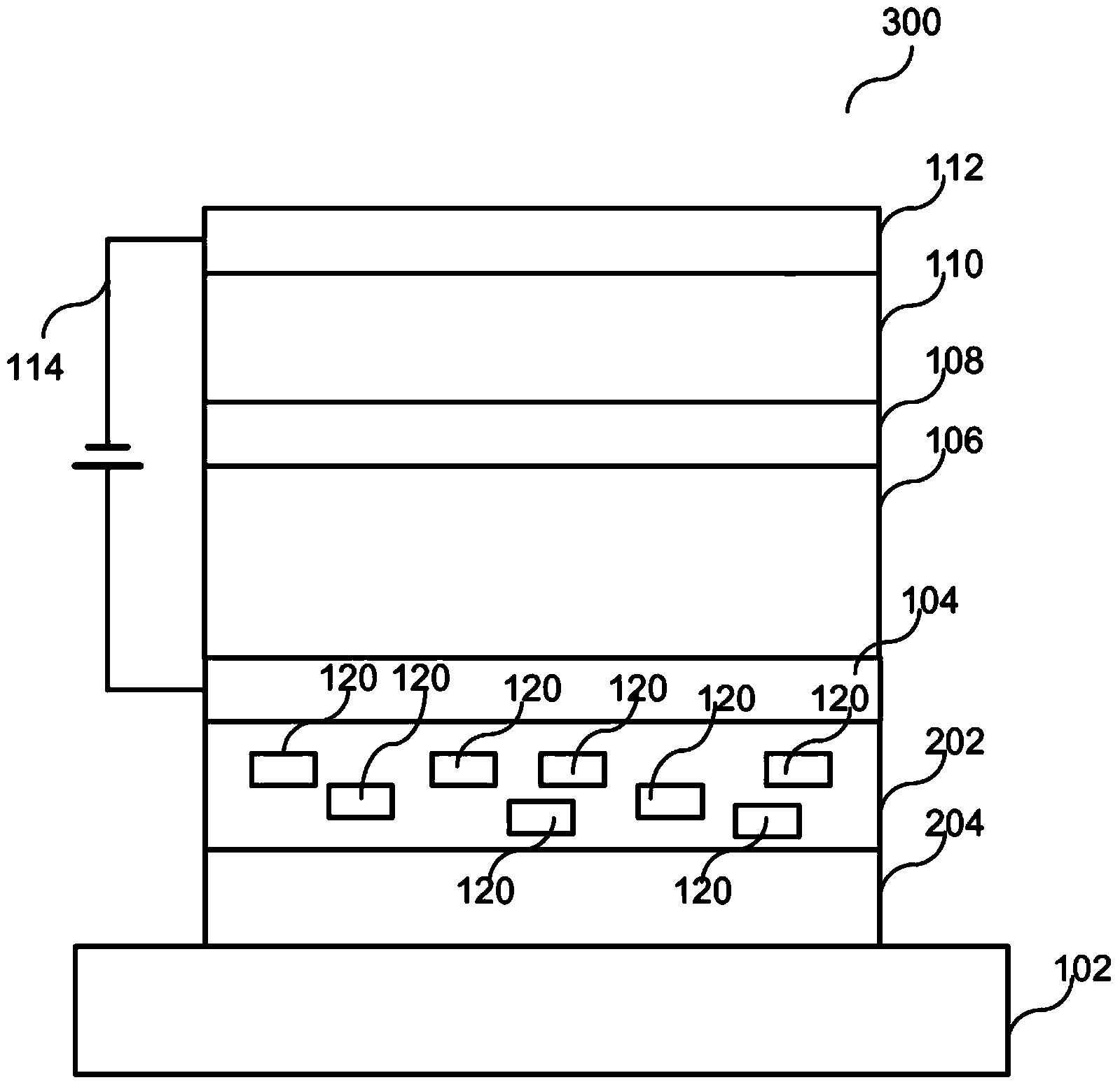
The invention relates to a light-emitting component (100) in various exemplary embodiments, comprising a first translucent electrode (104), an organic electroluminescent layer structure (106, 108) on or over the first electrode (104), a second translucent electrode (112) on or over the organic electroluminescent layer structure (106, 108), an optically translucent layer structure (116) on or over the second electrode (112), wherein the optically translucent layer structure (116) comprises a photoluminescence material (120), and a mirror layer structure (118) on or over the optically translucent layer structure (116).

Description

Technical field [0001] The present invention relates to a light emitting device and a method for manufacturing the light emitting device. Background technique [0002] In an organic light emitting diode (OLED), light is generated, for example, by means of electroluminescence of an organic color center (chromophore) in an organic matrix. The organic matrix is ​​usually located in a layer stack composed of an organic transport material and, for example, at least two conductive electrodes on a substrate. At least one of the two conductive electrodes is translucent, for example, transparent, and forms an optical microcavity together with the layer stack and the second conductive electrode, and forms an optical microcavity together with additional dielectric layers for optical matching if necessary. Microcavity, the dielectric layer can also be part of an organic light emitting diode. [0003] The choice of color centers and organic materials and the structure of the layer stack have ...

Claims


Application Information

Patent Timeline
Patent Type & Authority Applications(China)
IPC IPC(8): H01L51/52
CPCH01L51/5262H01L51/5271H01L27/322H01L51/5265H10K59/38H10K59/876H10K59/875H10K59/878H10K50/854H10K50/85H10K50/856H10K71/00H10K50/852
Inventor 托马斯·多贝廷埃尔温·兰蒂洛·罗伊施丹尼尔-斯特芬·塞茨
Owner OSRAM OLED
Learn More