
A kind of LED encapsulation structure of ESD protection and encapsulation method thereof

A technology of ESD protection and LED packaging, applied in the direction of electrical components, electrical solid devices, circuits, etc., can solve the problems of reducing LED luminous performance, high thermal resistance, affecting the conversion of electricity into light efficiency, etc., to reduce the risk of electrostatic breakdown, Effects of expanding application fields and improving design efficiency

Active Publication Date: 2016-03-30
JIANGYIN CHANGDIAN ADVANCED PACKAGING CO LTD
View PDF3 Cites 1 Cited by
  • Summary
  • Abstract
  • Description
  • Claims
  • Application Information

AI Technical Summary

Problems solved by technology

However, as a commercial product, the existing LED package still has the following defects: ①High thermal resistance
As we all know, the heat generated in turn affects the efficiency of electricity into light, thereby reducing the luminous performance of the LED itself
② LED chips are prone to electrostatic breakdown during the SMT process, and the traditional method of adding ESD electrostatic protection devices on the substrate can only help LED lamp beads reduce the risk of electrostatic breakdown after mounting

Method used


Image

  • A kind of LED encapsulation structure of ESD protection and encapsulation method thereof
  • A kind of LED encapsulation structure of ESD protection and encapsulation method thereof
  • A kind of LED encapsulation structure of ESD protection and encapsulation method thereof

Examples


Embodiment Construction

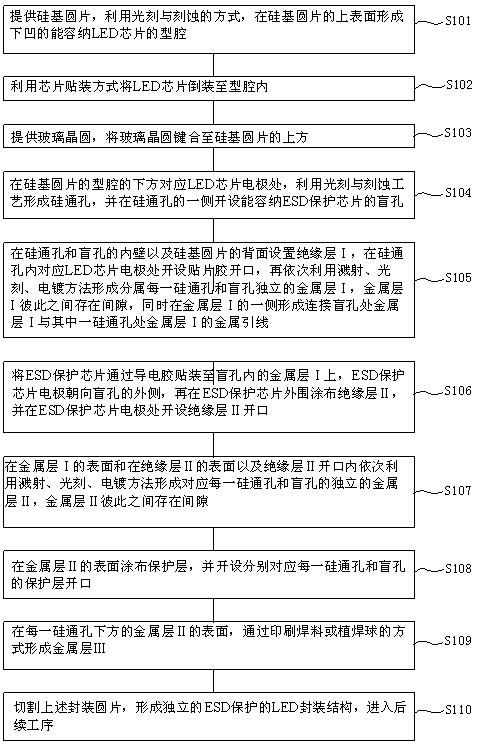
[0074] see figure 1 A kind of LED encapsulation method of ESD protection of the present invention comprises the following steps:

[0075] Executing step S101: providing a silicon-based wafer, and forming a concave cavity capable of accommodating LED chips on the upper surface of the silicon-based wafer by means of photolithography and etching;

[0076] Execute step S102: Flip-chip the LED chip into the cavity by chip mounting;

[0077] Executing step S103: providing a glass wafer, and bonding the glass wafer to the top of the silicon-based wafer;

[0078] Executing step S104: using photolithography and etching processes to form through-silicon vias at the corresponding LED chip electrodes under the cavity of the silicon-based wafer, and opening blind holes capable of accommodating ESD protection chips on one side of the through-silicon vias;

[0079] Step S105 is executed: an insulating layer I is provided on the inner wall of the through-silicon via and the blind via and th...


PUM


Abstract

The invention relates to an ESD (electronic static discharge) protected LED (light-emitting diode) packaging structure as well as a packaging method thereof, and belong to the technical field of semiconductor packaging. The ESD protected LED packaging structure comprises an LED chip (200) and an ESD protective chip (300), wherein the LED chip (200) is reversely installed in a cavity (111) of a silicon base body (110); the ESD protective chip (300) is embedded into a blind hole (113) in the other surface of the silicon base body (110); the LED chip (200) and the ESD protective chip (300) are electrically communicated and are electrically communicated with the external world by multi-layer metal layers in silicon through holes (112) below the cavity (111) and in the blind hole (113) as well as metal leads (900) connected with the multi-layer metal layers. The LED chip and the ESD electrostatic protective chip are integrated into a package body by the packaging structure realized by the invention; the ESD anti-electrostatic capability of the LED packaging structure is intensified; the packaging thermal resistance is reduced greatly by the addition of a heat radiation channel; the using performance of the LED chip is improved; the service life of the LED chip is prolonged.

Description

technical field [0001] The invention relates to an ESD-protected LED packaging structure and a packaging method thereof, belonging to the technical field of semiconductor packaging. Background technique [0002] Generally, the packaging of light-emitting diodes (Light-Emitting Diode, referred to as LED, the same below) has various packaging forms. In the early days, the lead frame was used as the substrate for packaging, and the LED chip was mounted on the lead frame through thermal paste (or conductive glue), and the current was loaded by wire bonding to make it emit light; with the advancement of technology, some new The emergence of high-quality, high-performance substrate materials has played a leading role in the application of high-power LEDs, such as ceramic substrates, AlN substrates, etc. However, as a commercial product, the existing LED package still has the following defects: ① high thermal resistance. Since the LED chip emits light through the electron recombi...

Claims


Application Information

Patent Timeline
Patent Type & Authority Patents(China)
IPC IPC(8): H01L33/48H01L33/62H01L33/64
CPCH01L2224/92244
Inventor 张黎赖志明陈栋陈锦辉
Owner JIANGYIN CHANGDIAN ADVANCED PACKAGING CO LTD
Learn More