An infrared gas sensor integrated with gas chamber packaging
A gas sensor and sensor technology, applied in instruments, measuring devices, scientific instruments, etc., can solve the problems of large gas chambers of MEMS infrared detectors
- Summary
- Abstract
- Description
- Claims
- Application Information
AI Technical Summary
Problems solved by technology
Method used
Image
Examples
Embodiment 1
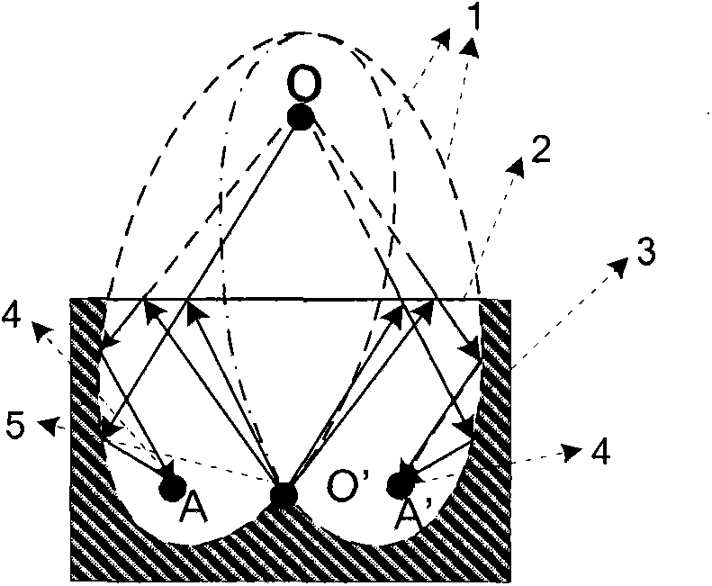
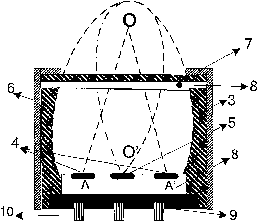
[0109] refer to figure 1 , is the air chamber structure and principle schematic diagram of the present invention, this air chamber comprises top plane 2, bottom plane and ellipse inner wall; The points are the two foci of the rotating ellipse, the light source 5 is located at the point O' on the bottom plane, and the point O' is symmetrical with the focus O on the reflective inner wall of the top plane 2 of the air chamber. In this way, from the point O' After the light emitted by the light source 5 is reflected by the inner wall of the ellipse, it is extended in reverse and intersects with the focal point O of the ellipse. According to the principle of elliptical optical propagation, the light emitted by the focal point is completely intersected with another focal point A or A' through the inner wall of the ellipse, which is the present invention The position of middle sensitive element 4. The rotating ellipse 1 rotates one circle along the vertical axis of rotation OO', tha...
Embodiment 2
[0114] refer to Figure 5 ,exist Figure 5 The shown infrared gas sensor for multi-gas detection includes four sensitive elements, which are respectively: a first sensitive element 51, a second sensitive element 52, a third sensitive element 53 and a reference sensitive element 54, and the four sensitive elements are all Distributed on the circle centered on the nano-surface modified infrared light source 56, wherein an L-shaped heat insulation channel 55 is set between the first sensitive element 51 and the second sensitive element 52, the third sensitive element 53 and the reference sensitive element An L-shaped heat insulation channel 55 is also set between 54; the four sensitive elements and the nano-surface modified infrared light source 56 are all thermally isolated from each other by a thermal isolation wall 57 to reduce the influence of thermal crosstalk.
[0115] Using MEMS technology, four gas infrared sensors and MEMS infrared light sources are prepared on a single...
Embodiment 3
[0117] Different from the infrared light source in Embodiment 1, this embodiment provides a nano-surface modified infrared light source 56. As a specific example, refer to Image 6 In steps (a)-(g), the preparation process of the nano-surface modified infrared light source 56 of the present invention is described in detail as follows:
[0118] (a), growing silicon nitride 62 on a single crystal silicon substrate 61, experimental conditions: temperature 780°C, 330mTorr, SiH 2 Cl 2 : 24 sccm, NH 3 : 90 sccm;
[0119] (b) Deposition of amorphous silicon 63: the temperature is 270°C, and the gas ratio is SIH 4 : 24% NH 3 : 55%N 2 :5.2% RF: 170:
[0120] (c), Al sputtering and annealing: magnetron sputtering Al, conditions: air pressure 10mTorr, after feeding Ar to meet the air pressure conditions, set RF to 8400W, and then perform annealing treatment at 450°C for 90 minutes;
[0121] (d) Wet etching of the Al film: using a conventional Al etching solution, Al-Si compound pa...
PUM
 Abstract
Description
Claims
Application Information
 - Generate Ideas
- Intellectual Property
- Life Sciences
- Materials
- Tech Scout
- Unparalleled Data Quality
- Higher Quality Content
- 60% Fewer Hallucinations
Browse by: Latest US Patents, China's latest patents, Technical Efficacy Thesaurus, Application Domain, Technology Topic, Popular Technical Reports.
© 2025 PatSnap. All rights reserved.Legal|Privacy policy|Modern Slavery Act Transparency Statement|Sitemap|About US| Contact US: help@patsnap.com


