Light-emitting diode packaging structure

A technology of light-emitting diodes and packaging structures, which is applied in the direction of semiconductor devices, electrical components, circuits, etc., and can solve the problems of reducing light-emitting performance of light-emitting diode packages, light transmittance drop, variability, etc.

Inactive Publication Date: 2016-10-05
中山晨溪光电科技有限公司
View PDF4 Cites 0 Cited by
  • Summary
  • Abstract
  • Description
  • Claims
  • Application Information

AI Technical Summary

Problems solved by technology

However, after being directly irradiated by short-wavelength (below 500 nm) light beams, bisphenol-A epoxy resins are highly susceptible to denaturation, resulting in a decrease in light transmittance, which ultimately affects the light extraction performance of the LED packaging structure and reduces the cost. Affected light extraction performance of light-emitting diode packages

Method used


Image

  • Light-emitting diode packaging structure
  • Light-emitting diode packaging structure
  • Light-emitting diode packaging structure

Examples


Embodiment Construction

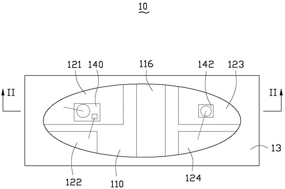
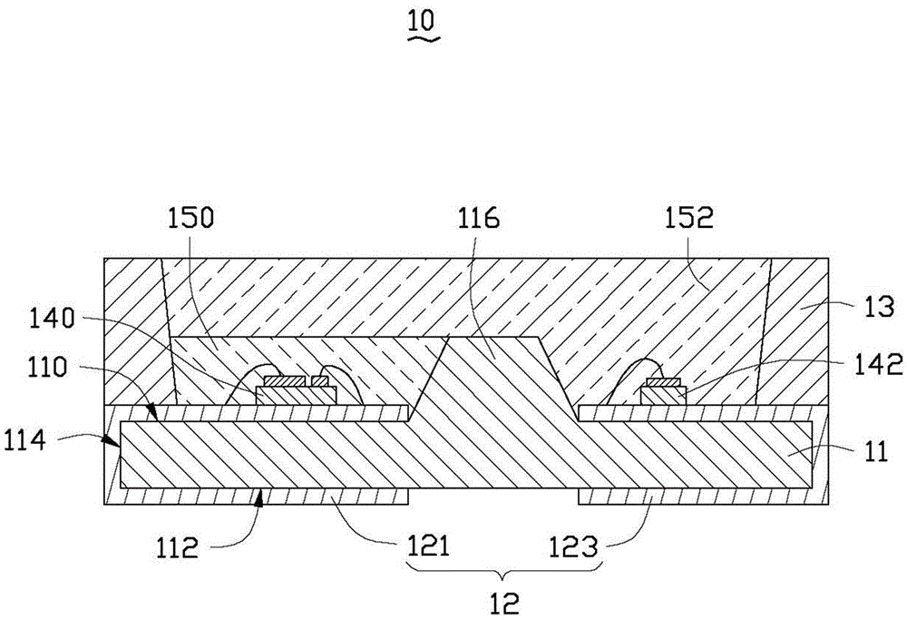
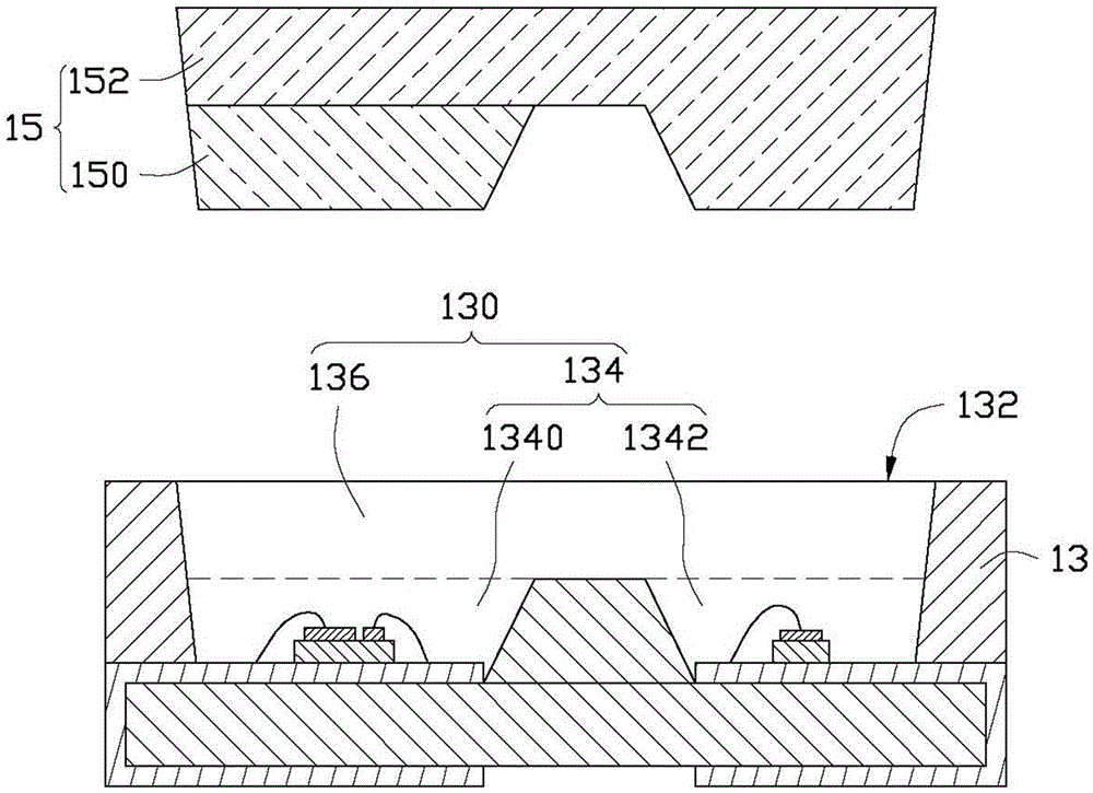
[0016] see figure 1 , figure 2 and image 3 , The light emitting diode package structure 10 provided by the first embodiment of the present invention includes a substrate 11 , electrodes 12 , reflective cups 13 , light emitting diode die 14 and a package body 15 .

[0017] The substrate 11 is an insulating substrate, and its material can be insulating materials such as sapphire (Sapphire) and silicon carbide (SiC). The substrate 11 includes a carrying surface 110 (ie figure 1 The upper surface of the substrate 11 shown), the bottom surface 112 opposite to the carrying surface 110, the side surface 114 located between the carrying surface 110 and the bottom surface 112 and connecting the carrying surface 110 and the bottom surface 112, and the side facing away from the bottom surface 112 from the carrying surface 110 The direction protruding stopper 116. The stopper 116 is located at the bottom of the reflection cup 13 . Preferably, the size of the stopper 116 gradually d...


PUM


Abstract

A light-emitting diode packaging structure, including a substrate, an electrode arranged on the substrate, a reflective cup, a light-emitting element, and a package body, the substrate is formed with a stopper at the bottom of the reflective cup, and the stopper separates the space at the bottom of the reflective cup into a first housing part and a second housing part that are not communicated with each other, the light-emitting element includes a first light-emitting diode die disposed in the first housing part and a second light-emitting diode die disposed in the second housing part, the first light-emitting diode The emission wavelength of a light emitting diode crystal grain is smaller than that of the second light emitting diode crystal grain, the first containing part is filled with cycloaliphatic epoxy resin, the second containing part and the head space of the reflective cup are filled with bisphenol A epoxy resin. This light-emitting diode packaging structure can take into account both good light extraction performance and low manufacturing cost.

Description

technical field [0001] The invention relates to a semiconductor structure, in particular to a light emitting diode packaging structure. Background technique [0002] Compared with traditional light sources, light emitting diodes (Light Emitting Diode, LED) have the advantages of light weight, small size, low pollution, long life, etc. As a new type of light source, it has been increasingly used in In various fields, such as street lights, traffic lights, signal lights, spotlights and decorative lights. [0003] Existing LED packaging structures generally include a substrate, electrodes on the substrate, LED chips carried on the substrate and electrically connected to the electrodes, and a package covering the LED chips on the substrate. In the packaging process of the light emitting diode, in order to reduce the cost, the low cost bisphenol A epoxy resin is usually used to cover the light emitting diode chip as the packaging body. However, after being directly irradiated b...

Claims


Application Information

Patent Timeline
Patent Type & Authority Patents(China)
IPC IPC(8): H01L25/075H01L33/56H01L33/48
CPCH01L2224/48091H01L2224/48137H01L2924/00014
Inventor 罗杏芬
Owner 中山晨溪光电科技有限公司
Why Eureka
Try Eureka