Trench IGBT and manufacturing method thereof

An insulated gate and channel technology, applied in the field of electronics, can solve the problems of accumulation layer channel type IGBT conduction voltage drop

Inactive Publication Date: 2014-01-01
PEKING UNIV FOUNDER GRP CO LTD +1
View PDF6 Cites 0 Cited by
  • Summary
  • Abstract
  • Description
  • Claims
  • Application Information

AI Technical Summary

Problems solved by technology

[0004] Although the existence of the accumulation layer channel reduces the conduction voltage drop of the accumulation layer channel type IGBT, it cannot make the conduction voltage drop of the accumulation layer channel type IGBT lower

Method used


Image

  • Trench IGBT and manufacturing method thereof
  • Trench IGBT and manufacturing method thereof
  • Trench IGBT and manufacturing method thereof

Examples


Embodiment Construction

[0026] Compared with the existing Trench IGBT, the conduction voltage drop of the Trench IGBT provided by the invention is greatly reduced.

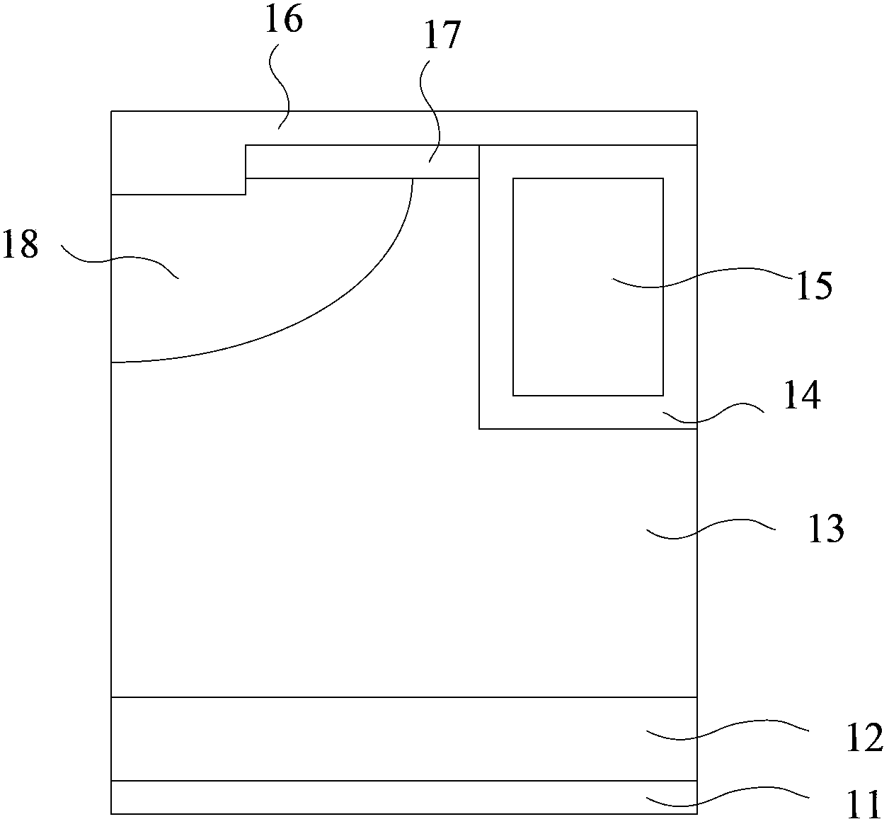
[0027] The Trench IGBT structure in the embodiment of the present invention will be described below with reference to the accompanying drawings. Such as figure 2 As shown, the Trench IGBT in this embodiment includes: a metalized anode 21, a P-type heavily doped region 22, an N-type low-doped substrate base region 23, a gate oxide layer 24, a gate electrode 25, a metalized cathode 26, Cathode metal Schottky contact layer 27 and Pbody withstand voltage region 28 .

[0028] Among them, the P-type heavily doped region 22 is in contact with the metallized anode 21, the N-type low-doped substrate base region 23 is in contact with the P-type heavily doped region 22, and the gate oxide layer 24 is in contact with the N-type low-doped substrate base region. 23, the gate electrode 25 is in contact with the gate oxide layer 24, the Pbody withsta...


PUM


Abstract

The invention provides a Trench IGBT and a method for manufacturing the Trench IGBT. A Schottky contact structure is adopted in the Trench IGBT, and the conductivity voltage drop of the Trench IGBT is reduced. The Trench IGBT comprises a gate oxide layer, a Pbody voltage withstanding area, and an N-type low-adulteration substrate base area, a metallization cathode and a Schottky contact layer which is located between the gate oxide layer and the Pbody voltage withstanding area and is in contact with the N-type low-adulteration substrate base area and the metallization cathode. The method for manufacturing the Trench IGBT comprises the steps that after the Pbody voltage withstanding area and the gate oxide layer are formed on the N-type low-adulteration substrate base area, the Schottky contact layer is formed on the N-type low-adulteration substrate base area between the gate oxide layer and the Pbody voltage withstanding area; the metallization cathode is formed on the Schottky contact layer.

Description

technical field [0001] The invention relates to the field of electronic technology, in particular to a channel type insulated gate bipolar transistor and a manufacturing method thereof. Background technique [0002] The emergence of Trench IGBT (Trench Insulated Gate Bipolar Transistor, trench-type insulated gate bipolar transistor) has enhanced reliability compared with ordinary IGBTs and reduced parasitic thyristor effects. The channel type IGBT controlled by the accumulation layer has greater advantages than the conventional IGBT, and its structure is as follows figure 1 As shown, it includes metallized anode 11, P-type heavily doped region anode 12, N-type lightly doped substrate base region 13, gate oxide layer 14, gate electrode 15, metallized cathode 16, N-type heavily doped region 17. Pbody pressure zone 18. [0003] The existing Trench IGBT controls the blocking of the device through the electronic barrier formed by the built-in electric field of the front P-type ...

Claims


Application Information

Patent Timeline
Patent Type & Authority Applications(China)
IPC IPC(8): H01L29/47H01L29/739H01L21/331
CPCH01L29/7397H01L29/401H01L29/47H01L29/66348
Inventor 方伟
Owner PEKING UNIV FOUNDER GRP CO LTD
Why Eureka
Try Eureka