Array substrate, color film substrate and display device
A technology of array substrates and color film substrates, which is applied in optics, instruments, electrical components, etc., can solve the problems of excessive viewing angles of displays and the inability of displays to meet narrow viewing angles, and achieve the effect of reducing viewing angles
- Summary
- Abstract
- Description
- Claims
- Application Information
AI Technical Summary
Problems solved by technology
Method used
Image
Examples
Embodiment 1
[0036] An embodiment of the present invention provides an array substrate, including a plurality of pixel units distributed in a matrix, and a light concentrating element is provided in the display area of each pixel unit, and the display area is a light-transmitting area or a light-emitting area of each pixel unit , the light concentrating element is arranged on the light output path of the array substrate.
[0037] In the array substrate in this embodiment, since the display area of each pixel unit is provided with a light-condensing element, the outgoing light needs to pass through the light-condensing element, and the refractive index of the light-condensing element is relatively large, so that the outgoing light has a smaller The angle is emitted from the light-emitting surface of the array substrate, which has the effect of concentrating the emitted light, thereby reducing the viewing angle of the display device and realizing the protection of personal privacy or bu...
Embodiment 2
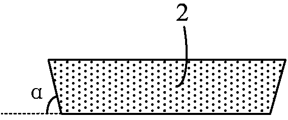
[0039] On the basis of Embodiment 1, this embodiment provides an array substrate for OLED display devices, such as figure 1 As shown, the array substrate further includes a medium layer adjacent to the above-mentioned light-condensing elements 2 , the medium layer is located between adjacent light-condensing elements 2 , and the refractive index of the light-condensing elements 2 is greater than the refractive index of the medium layer. The array substrate also includes: a plurality of OLED light emitting units 1 arranged in a plurality of pixel units, and each light concentrating element 2 is arranged between each OLED light emitting unit 1 and the light emitting surface of the array substrate.
[0040] Specifically, the array substrate includes a first substrate 31, a thin film field effect transistor (Thin Film Transistor, TFT) is disposed on the first substrate 31, a first protection layer 41 is disposed on the TFT, and the first protection layer 41 is used to protect the ...
Embodiment 3
[0049] On the basis of Embodiment 1, this embodiment provides an array substrate, the array substrate is an array substrate of a liquid crystal display, such as Figure 7 As shown, different from the OLED display device in Embodiment 2, in the liquid crystal display device, the outgoing light is provided through the backlight module under the array substrate, so the array substrates are all located on the light exit path, and the light concentrating element 2 can be arranged on the array substrate In any layer above, as long as each light concentrating element 2 is located in the display area of each pixel unit. Specifically, the array substrate includes a first substrate 31 on which pixel electrodes ( Figure 7 not shown in ) and the light-gathering element 2, the light-gathering element 2 can be arranged above or below the pixel electrode; the pixel unit on the color filter substrate includes a color resin 7 and a black matrix 8, the black matrix 8 is used to block light, ...
PUM
 Abstract
Description
Claims
Application Information
 - R&D Engineer
- R&D Manager
- IP Professional
- Industry Leading Data Capabilities
- Powerful AI technology
- Patent DNA Extraction
Browse by: Latest US Patents, China's latest patents, Technical Efficacy Thesaurus, Application Domain, Technology Topic, Popular Technical Reports.
© 2024 PatSnap. All rights reserved.Legal|Privacy policy|Modern Slavery Act Transparency Statement|Sitemap|About US| Contact US: help@patsnap.com


