
A new type of silicon nanomaterial solar cell and its preparation method

A technology of solar cells and new structure, applied in the field of solar cells, can solve the problems of complex preparation process of solar cells, photoelectric conversion efficiency to be improved, difficulty in production and the like

Inactive Publication Date: 2015-12-02
SUZHOU UNIV
View PDF3 Cites 0 Cited by
  • Summary
  • Abstract
  • Description
  • Claims
  • Application Information

AI Technical Summary

Problems solved by technology

[0005] The above-mentioned solar cells based on the p-n junction structure are complex and difficult to manufacture, and the photoelectric conversion efficiency needs to be improved.

Method used

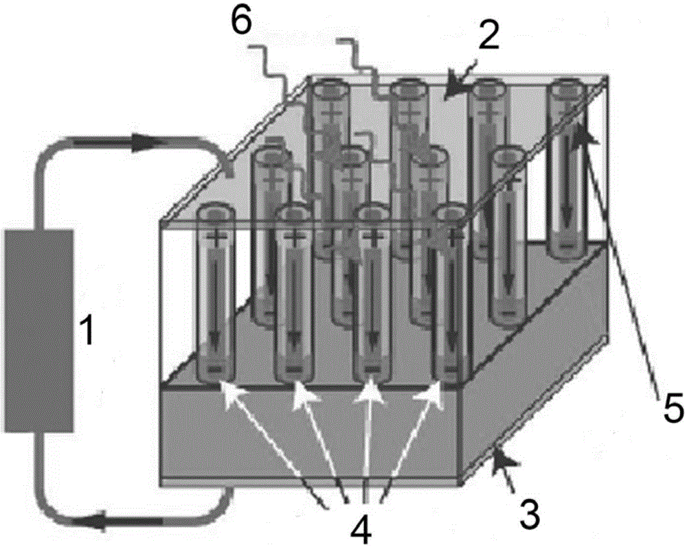

Image

  • A new type of silicon nanomaterial solar cell and its preparation method

Examples


Embodiment 1

[0030] Put a 5 mm × 5 mm heavily doped silicon wafer in a plastic cup, add 10 ml of ethanol hydrofluoric acid solution with a mass fraction of 5%, and then add silver nitrate solid to obtain a silver nitrate solution with a concentration of 0.1 mol / L. React at 50°C for 2 hours to obtain silicon nanowires, heat the obtained silicon wafer with silicon nanowires in a muffle furnace at 900°C for 5 minutes, use oxygen in the air to partially oxidize the silicon nanowires, and generate a built-in electric field , take out the silicon wafer from the muffle furnace, set the bottom electrode on the bottom of the silicon wafer, the bottom electrode is in ohmic contact with the surface of the silicon wafer, spin coat a layer of conductive glue on the upper part of the silicon wafer (the side with silicon nanowires), and then steam Transparent electrodes, solar cells can be prepared after packaging, and the efficiency can reach 10%.

Embodiment 2

[0032] 20 mg of silicon nanoparticles (purchased from Aldrich, particle size less than 100 nm, CAS No.: 7440-21-3) were irradiated under synchrotron radiation for 1 hour to generate a built-in electric field, and then dispersed in 50 ml of water, Assemble under the action of an electric field or a magnetic field, then spin-coat the suspension on ITO glass, spin-coat the conductive glue after drying, steam the metal electrodes, and package it to make a solar cell with an efficiency of up to 10%.

Embodiment 3

[0034] 20 mg of silicon nanoparticles (purchased from Aldrich with a particle size of less than 100 nm, CAS No.: 7440-21-3) were irradiated with alpha rays for 2 hours to generate a built-in electric field, and then dispersed in 50 ml of dodecyl In the aqueous solution of sodium benzenesulfonate, after being assembled into a film, move it to ITO glass, spin-coat the conductive glue after drying, steam the metal electrode, and package it to make a solar cell with an efficiency of up to 10%.


PUM


Abstract

The invention relates to a silicon nanomaterial solar cell with a new structure and a preparation method thereof. The silicon nanomaterial solar cell with the novel structure includes top electrodes arranged sequentially from top to bottom, modified ones with piezoelectric effect and capable of generating inner electrodes. Silicon nanomaterials and bottom electrodes that build an electric field. The present invention does not rely on traditional p-n Instead, silicon nanomaterials are prepared first, then modified to generate a built-in electric field, and then silicon nanomaterials are assembled into films or arrays, and then electrodes are evaporated to form solar cells with an efficiency of up to 10% . The invention does not need to use high-purity silicon material, greatly reduces the cost, and has good application.

Description

technical field [0001] The invention relates to the technical field of solar cells, in particular to a silicon nanomaterial solar cell with a novel structure and a preparation method thereof. Background technique [0002] Traditional solar cells are based on the p-n junction structure, such as the patent (201110143760.4) polycrystalline silicon nanowire solar cell and its preparation method applied by Shanghai Jiaotong University on May 31, 2011. The polycrystalline silicon nanowire solar cell includes: from top to bottom Composite layer gate electrode, transparent ITO conductive film layer, silicon nitride passivation anti-reflection layer, n-type silicon nanowire array, p-type silicon substrate and metal back electrode, transparent ITO conductive film layer, silicon nitride passivation anti-reflection layer Both the reflective layer and the n-type silicon nanowire array have a square-wave structure. After etching the p-type polycrystalline silicon wafer with a mixed soluti...

Claims


Application Information

Patent Timeline
Patent Type & Authority Patents(China)
IPC IPC(8): H01L31/0216H01L31/052H01L41/18H01L41/25H01L31/18
CPCY02E10/50Y02P70/50
Inventor 邵名望尹奎李述汤
Owner SUZHOU UNIV
Learn More