A kind of preparation method of polycrystalline silicon surface micro-nano composite structure

A micro-nano composite structure, polysilicon technology, applied in the application field, can solve the problems of poor repeatability, serious surface compounding, and high consumption of precious metals.

Active Publication Date: 2020-07-07
LUDONG UNIVERSITY
View PDF5 Cites 0 Cited by
  • Summary
  • Abstract
  • Description
  • Claims
  • Application Information

AI Technical Summary

Problems solved by technology

[0004] The invention can solve the problems of large consumption of precious metals, serious surface recombination, poor compatibility of optical properties and electrical properties, disordered micro-nano structures, poor repeatability, and difficult human control in the existing polycrystalline black silicon suede surface wet preparation technology, and provides a Preparation method of micro-nano composite structure on polycrystalline silicon surface

Method used


Image

  • A kind of preparation method of polycrystalline silicon surface micro-nano composite structure

Examples


specific Embodiment approach

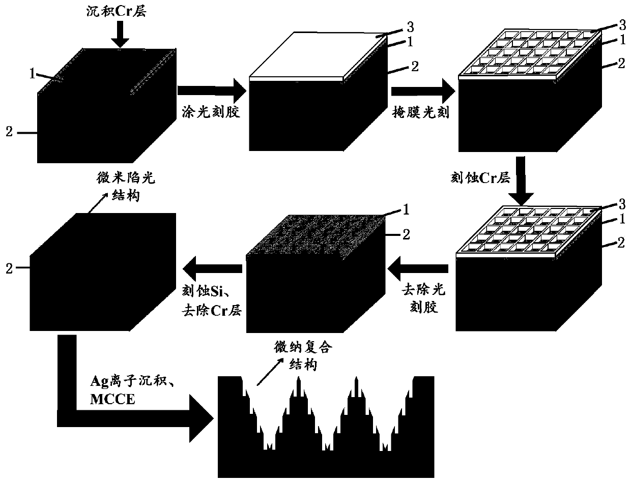
[0014] Specific embodiments: a method for preparing a micro-nano composite structure on the surface of polysilicon, which is completed by the following steps:

[0015] Step 1: the deposition of Cr metal film on the surface of polycrystalline silicon wafer, the steps are as follows: take a polycrystalline silicon wafer sliced ​​by a diamond wire, clean it with absolute ethanol and deionized water, utilize the magnetron sputtering method to coat metal Cr film on polycrystalline silicon wafer, select The high-purity Cr target is used as the sputtering target, and the polysilicon wafer is placed in the vacuum chamber, and the vacuum is first drawn. When the vacuum degree of the equipment is 3.0×10 -5 At Torr, start the Cr target, and then pass in argon gas for 30min ion cleaning; after the ion cleaning process, control the target current to 1A, the substrate bias voltage to 75V, and the gas flow rate to 20sccm for Cr film deposition. By adjusting the deposition time, the polysilico...


PUM


Abstract

The invention discloses a preparation method of a micro-nano composite structure on the surface of polycrystalline silicon, in particular to the technical fields of micro-processing and solar cells. At first, a lay of metal Cr film is deposited on the surface of a polycrystalline silicon wafer, and then photolithography and etching are carried out on the Cr film to fabricate a micron Cr metal maskpattern; then the silicon wafer is etched by a silicon wafer etching solution to obtain the micrometer trapped structure, and the remaining Cr film is removed by Cr etching solution to obtain the micrometer trapped structure on the surface of polysilicon. Finally, Ag ions are deposited on the surface of silicon wafer, and the nanostructures are prepared by metal catalytic chemical etching of Ag ions. After removing the residual Ag ions, the micro-nano composite structure is obtained. Compared with the conventional black silicon pile surface preparation technology, the preparation method of the invention can effectively reduce the consumption of noble metals, can avoid additional surface recombination, and the shape period of the micro-nano composite structure is controllable, so that theabsorption of sunlight by the polycrystalline silicon wafer can be greatly increased on the premise of giving consideration to the electrical performance.

Description

technical field [0001] The invention relates to application fields such as microfabrication and solar cell technology, and in particular to a method for preparing a micro-nano composite structure on the surface of polycrystalline silicon. Background technique [0002] The current methods for preparing polycrystalline black silicon at home and abroad can be roughly divided into two categories: dry etching and wet etching. Dry etching is to use reactive gas or plasma for etching, mainly including femtosecond laser pulse etching and reactive ion etching, among which there are many researches on reactive ion etching; wet etching is to use chemical The chemical reaction between the reagent and the material to be etched is carried out, and the typical preparation method is the metal-catalyzed chemical etching method. Reactive ion etching technology uses the active reactive groups generated by the plasma to chemically react with the material to be etched. At the same time, physica...

Claims


Application Information

Patent Timeline
Patent Type & Authority Patents(China)
IPC IPC(8): H01L31/18
CPCH01L31/182Y02E10/546Y02P70/50
Inventor 张登英赵风周张立春许家沛黄玉鹏罗兴
Owner LUDONG UNIVERSITY
Why Eureka
Try Eureka