Novel double-layer-film back-passivated solar cell structure
A solar cell and rear passivation technology, which is applied in circuits, electrical components, semiconductor devices, etc., can solve the problems of limiting the popularization of selective emitter batteries, and achieve the effects of improving passivation effect, spectral response, and absorption
- Summary
- Abstract
- Description
- Claims
- Application Information
AI Technical Summary
Problems solved by technology
Method used
Image
Examples
Embodiment Construction
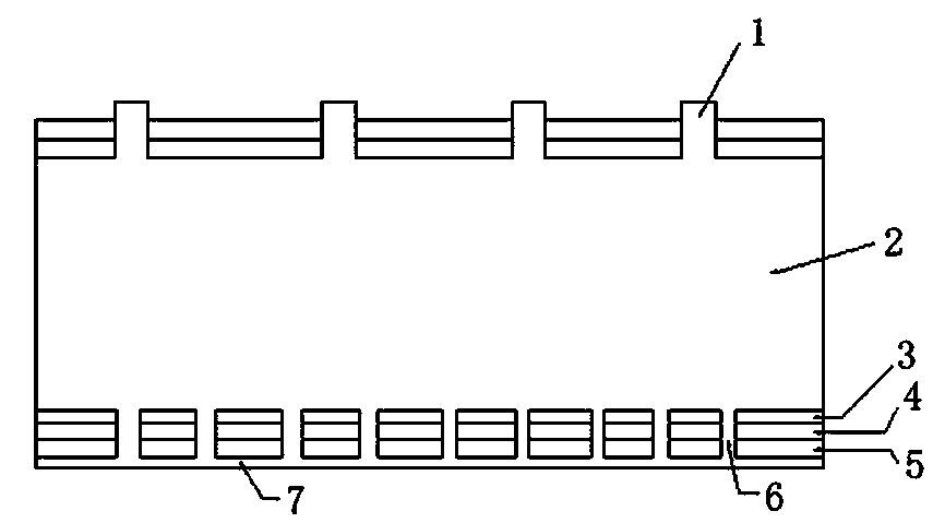
[0011] Such as figure 1 As shown, a new double-layer film back passivation solar cell structure, including silver electrode 1, silicon nitride dielectric film 5, aluminum back field 7, P-type silicon substrate 2, deposited on the silicon nitride dielectric film 5 Aluminum oxide passivation film 3 and silicon oxynitride passivation film 4, and grooves 6 are evenly distributed on the back field of silicon nitride dielectric film 5, aluminum oxide passivation film 3 and silicon oxynitride passivation film 4. The thickness of the aluminum oxide passivation film 3 is in the range of 10-20 nm, and the thickness of the silicon oxynitride passivation film is in the range of 15-25 nm.
PUM
| Property | Measurement | Unit |
|---|---|---|
| thickness | aaaaa | aaaaa |
| thickness | aaaaa | aaaaa |
| thickness | aaaaa | aaaaa |
Abstract
Description
Claims
Application Information
 - R&D
- Intellectual Property
- Life Sciences
- Materials
- Tech Scout
- Unparalleled Data Quality
- Higher Quality Content
- 60% Fewer Hallucinations
Browse by: Latest US Patents, China's latest patents, Technical Efficacy Thesaurus, Application Domain, Technology Topic, Popular Technical Reports.
© 2025 PatSnap. All rights reserved.Legal|Privacy policy|Modern Slavery Act Transparency Statement|Sitemap|About US| Contact US: help@patsnap.com

