
LED chip oblique cutting method, LED light-emitting element and LED lighting device

A LED chip, oblique cutting technology, applied in the direction of electrical components, electrical solid devices, semiconductor/solid device manufacturing, etc., can solve the problems of high comprehensive cost, high complexity, and infeasibility, so as to improve efficiency, reduce heat loss, Effect of Luminous Efficiency Improvement

Inactive Publication Date: 2016-12-07
陈枕流
View PDF5 Cites 0 Cited by
  • Summary
  • Abstract
  • Description
  • Claims
  • Application Information

AI Technical Summary

Problems solved by technology

In addition to complex process operations, (for example, so many chips (such as 25×25 micron chips generally require mounting 1600pis / 1W) must be solidified in the mounting process, wire bonding, phosphor powder, and glue. , although they are all completed by high-speed automatic machinery, but the complexity is high and the overall cost is higher, which directly affects the entry of LED into the field of white light general lighting), and the more difficult problem is the photon side of the 1×1mil (about 25×25 microns) chip The ratio of the area to the lead-out area on the front of the chip is still too small (see Figure 5 of the above-mentioned background technology patent document). Further reducing the chip design area can further improve the light efficiency, but the thickness of the microcrystalline chip is 3 to 4 microns, which is relatively small for 1 For a ×1mil (about 25×25 micron) chip, the side area is only 350 square microns, accounting for only 28% of 25×25×2=1250 square microns; if further improvement of photon extraction efficiency is considered, the size of the chip must be reduced. The ratio of the side lead-out area is greater than that of the front; but in terms of process cost, even the technically feasible cost is not feasible

Method used


Image

  • LED chip oblique cutting method, LED light-emitting element and LED lighting device
  • LED chip oblique cutting method, LED light-emitting element and LED lighting device
  • LED chip oblique cutting method, LED light-emitting element and LED lighting device

Examples


Embodiment Construction

[0020] Embodiments of the present invention will be described below with reference to the accompanying drawings. The same reference numerals denote the same parts in the drawings.

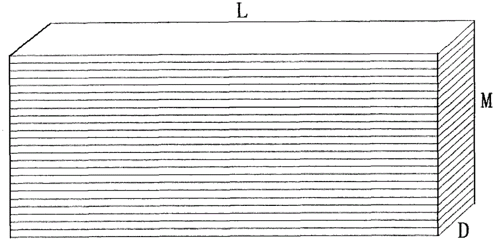
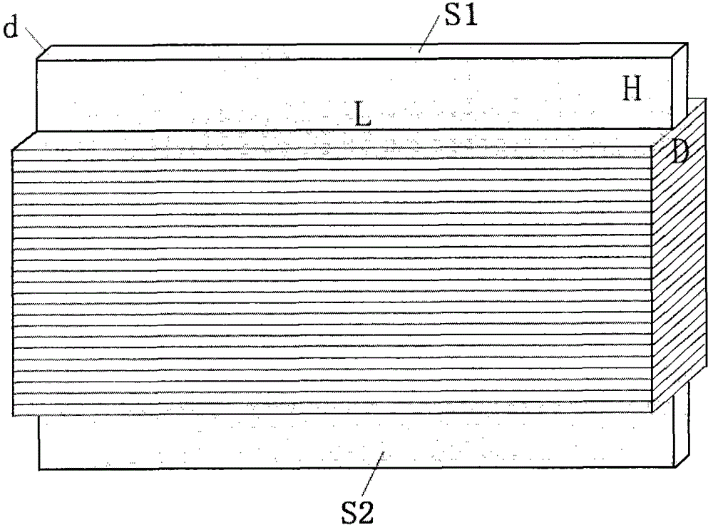
[0021] First, select n (n is an integer greater than 1) LED chips of the same type and remove the substrate of each LED chip. refer to figure 1 As shown, the substrate is first peeled off for large-sized chips. If the symbol P in the figure represents a P-type semiconductor material layer and the symbol N represents an N-type semiconductor material layer, an active light-emitting layer A is formed at the contact surface of the two layers. That is, the commonly known pn junction layer, which emits light in the case of forward conduction. Subsequently, a transparent electrode layer with a thickness of about 1.5 microns is directly bonded on both sides by epitaxy technology or crystal expansion technology, such as transparent Al 2 o 3 electrode layer. exist figure 1 The transparent electrode lay...


PUM


Abstract

The invention discloses an LED chip miter cutting and connecting method, an LED luminous element and an LED lighting device. The LED chip miter cutting method is characterized by comprising the steps of, during LED chip miter cutting, selecting n (n is an integer larger than 1) LED chips of the same type and removing a substrate of each LED chip, connecting PN junctions of the n LED chips with the substrates removed in series through transparent electrodes and bonding the LED chips into an LED chip lamination body, conducting miter cutting on the LED chip lamination body according to a preset angle alpha between the lamination body and a lamination plate to obtain an LED chip with the luminous face expanded, and encapsulating the LED chip with the luminous face expanded.

Description

technical field [0001] The invention relates to LED lighting technology. Specifically, the present invention relates to a method for cutting and connecting LED chips, an LED light-emitting element made by the cutting and connecting method, and an illuminating device composed of the LED light-emitting element. Background technique [0002] The LED photon extraction method and its extraction efficiency determine the use efficiency and application prospects of lighting devices using LEDs as light sources. Whether the LEDs in the prior art are packaged in millimeter (mm) or micron (μm) level chips, since the path of photons escaping from the active layer of the LED to the space is very complicated, transmission, reflection and absorption will occur during the escape process. And so on, photons are lost in every step of its conduction journey. Therefore, although the internal quantum efficiency of LEDs can reach 100%, the theoretical luminous efficiency reaches about 360lm / W; h...

Claims


Application Information

Patent Timeline
Patent Type & Authority Patents(China)
IPC IPC(8): H01L21/304H01L33/00H01L25/075
Inventor 陈枕流居家奇
Owner 陈枕流
Learn More