A kind of multi-junction solar cell with metal reflector and its preparation method
A technology of solar cells and metal reflectors, applied in the field of solar photovoltaics, can solve problems such as difficult operation, and achieve the effects of simple operation, increased utilization, and improved light utilization
- Summary
- Abstract
- Description
- Claims
- Application Information
AI Technical Summary
Problems solved by technology
Method used
Image
Examples
Embodiment 1
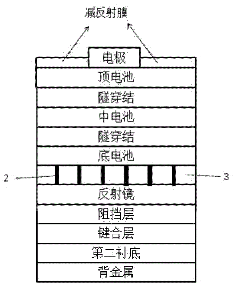
[0053] Embodiment 1, the fabrication method of the GaInP / GaAs / InGaNAs triple-junction solar cell with metal reflector, the steps are as follows:
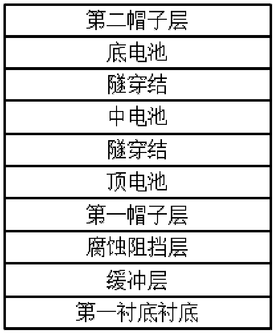
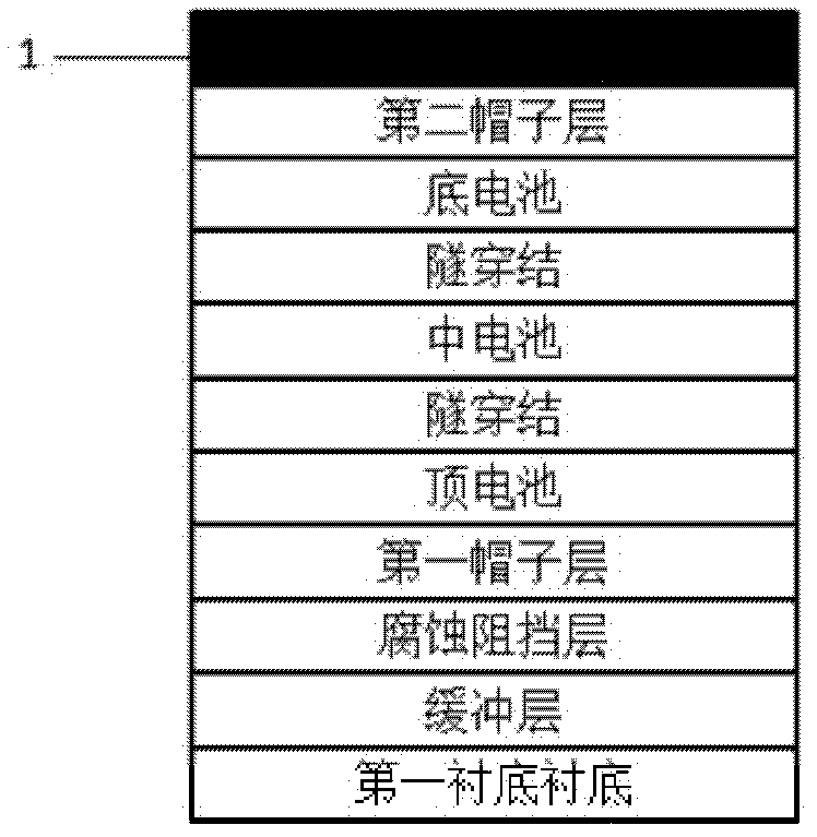
[0054] (1) The triple-junction solar cell epitaxial wafer is grown by MOCVD method, and the epitaxial wafer structure is as follows figure 1 As shown, the top cell GaInP, the middle cell GaAs, and the bottom cell InGaNAs are grown on the first substrate GaAs; the band gap of the top cell is larger than that of the middle cell, and the band gap of the middle cell is larger than that of the bottom cell.
[0055] (2) On the epitaxial wafer grown in step (1), clean the solar cell epitaxial wafer to remove surface organic matter and dirt, and vapor-deposit an ohmic contact NiAu metal layer on the surface of the second cap layer, and the thickness of NiAu is 1500 angstroms.
[0056] (3) On the basis of step (2), the current channel pattern is photolithographically formed, the figure is a frame rectangle figure, and the current channel are...
Embodiment 2
[0069] Embodiment 2, a kind of double-junction GaInP / GaAs solar cell manufacturing method with metal reflector, the steps are as follows:
[0070] (1) The double-junction solar cell epitaxial wafer is grown by MOCVD method, and the epitaxial wafer structure is as follows Figure 4 As shown, the top cell GaInP is first grown on the first substrate GaAs, and then the bottom cell GaAs is grown; the band gap of the top cell is larger than that of the bottom cell.
[0071] (2) cleaning the solar cell epitaxial wafer in step (1), removing surface organic matter and dirt, and vapor-depositing an ohmic contact GeAu metal layer on the surface of the second cap layer with a thickness of 3000 angstroms.
[0072] (3) On the basis of step (2), the photoetching current channel pattern, the pattern is a back-shaped pattern, and the current channel area is 5%-20% of the battery area. After the current channel pattern is corroded, the etching solution uses hydrogen peroxide: ammonia water: Wa...
PUM
| Property | Measurement | Unit |
|---|---|---|
| thickness | aaaaa | aaaaa |
| thickness | aaaaa | aaaaa |
| thickness | aaaaa | aaaaa |
Abstract
Description
Claims
Application Information
 - R&D
- Intellectual Property
- Life Sciences
- Materials
- Tech Scout
- Unparalleled Data Quality
- Higher Quality Content
- 60% Fewer Hallucinations
Browse by: Latest US Patents, China's latest patents, Technical Efficacy Thesaurus, Application Domain, Technology Topic, Popular Technical Reports.
© 2025 PatSnap. All rights reserved.Legal|Privacy policy|Modern Slavery Act Transparency Statement|Sitemap|About US| Contact US: help@patsnap.com


