Display panel, manufacturing method thereof, and display device
A display panel and display area technology, which is applied in the direction of instruments, optics, nonlinear optics, etc., can solve the problems of peeling off the sealing glue, low mechanical strength of the upper alignment layer of the alignment film, poor display of the display panel, etc., and achieve good display effect Effect
- Summary
- Abstract
- Description
- Claims
- Application Information
AI Technical Summary
Problems solved by technology
Method used
Image
Examples
Embodiment 1
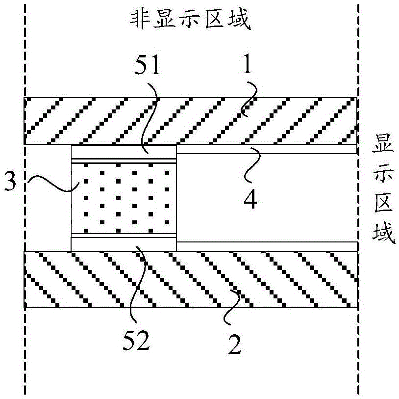
[0054] Please refer to image 3 , image 3 It is a schematic structural diagram of a display panel provided by the present invention. The present invention provides a display panel with a display area and a non-display area. The display panel includes: a first substrate 1 and a second substrate 2 oppositely arranged, and a A layer of liquid crystal molecules between the first substrate 1 and the second substrate 2, the first substrate 1 and the second substrate 2 are provided with an alignment film 4 at the position corresponding to the display area, and are provided with an alignment film 4 at the position corresponding to the non-display area. Frame sealant area 3 of the frame sealant,
[0055] The sealant area 3 of the surface of the first substrate 1 facing the liquid crystal molecular layer is provided with a first lifting layer 51, and the first lifting layer 51 makes the sealant area 3 of the first substrate 1 higher than its display area;
[0056] The sealant area 3 ...
Embodiment 2
[0069] Please refer to Figure 6 , Figure 6 The flow chart of the manufacturing method of the display panel provided by the present invention, the embodiment of the present invention provides a manufacturing method of the display panel, the display panel has a display area and a non-display area, and the first substrate and the second substrate corresponding to the non-display area The substrates respectively have a sealant area for coating the sealant, including:
[0070] Step S101: forming a first lifting layer pattern on the frame sealant area of the first substrate, so that the frame sealant area of the first substrate is higher than the display area of the first substrate;
[0071] Step S102: forming a second lifting layer pattern on the frame sealant area of the second substrate, so that the frame sealant area of the second substrate is higher than the display area of the array substrate;
[0072] Step S103: forming an alignment film on the display area of...
Embodiment 3
[0078] On the basis of Example 2, please continue to refer to Figure 4 , the method for manufacturing a display panel in which the first substrate is a color filter substrate and the second substrate is an array substrate is taken as an example for illustration, but not limited thereto.
[0079] Step S101 forms a first lifting layer pattern on the frame sealant area of the first substrate, so that the frame sealant area of the first substrate is higher than the display area of the first substrate (the first substrate 1 is a color filter substrate as an example for detailed description ) specifically include:
[0080] Forming a red color resist layer pattern 11 in the sealant area of the color filter substrate;
[0081] Forming a green color-resist layer pattern 12 on the red color-resist layer pattern 11;
[0082] Forming a blue color-resist layer pattern 13 on the green color-resist layer pattern 12;
[0083] The red color-resist layer pattern 11 , the green color...
PUM
 Abstract
Description
Claims
Application Information
 - R&D
- Intellectual Property
- Life Sciences
- Materials
- Tech Scout
- Unparalleled Data Quality
- Higher Quality Content
- 60% Fewer Hallucinations
Browse by: Latest US Patents, China's latest patents, Technical Efficacy Thesaurus, Application Domain, Technology Topic, Popular Technical Reports.
© 2025 PatSnap. All rights reserved.Legal|Privacy policy|Modern Slavery Act Transparency Statement|Sitemap|About US| Contact US: help@patsnap.com


