
Light-shielding composition, method for producing a light-shielding composition, solder resist, method for forming a pattern, and solid-state imaging device

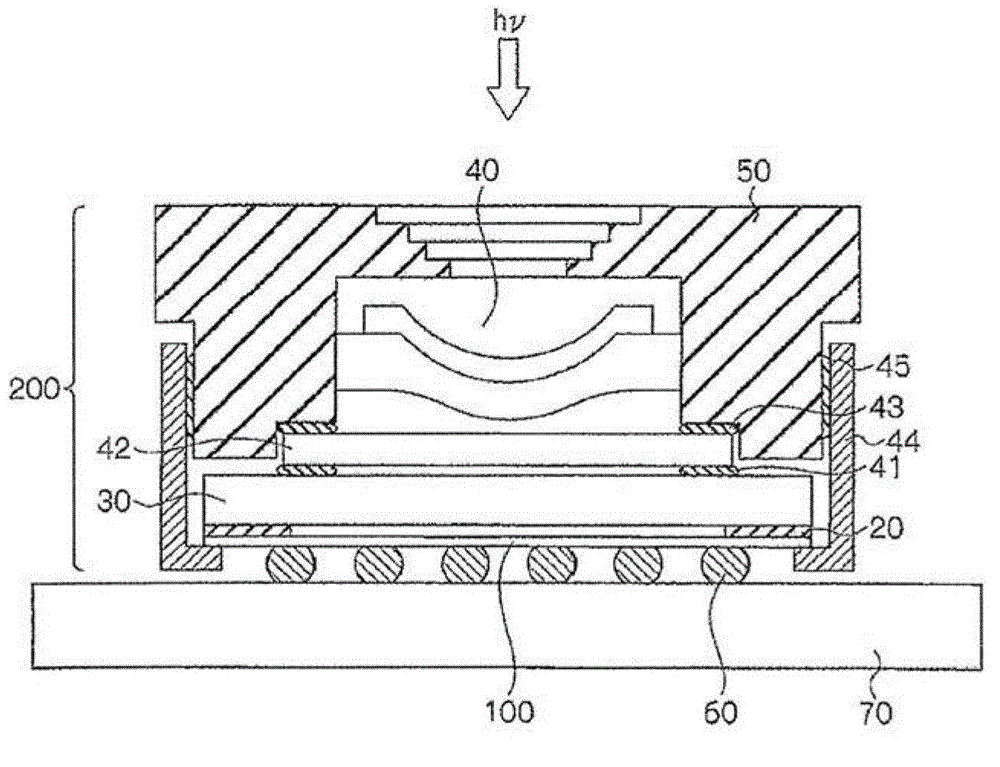
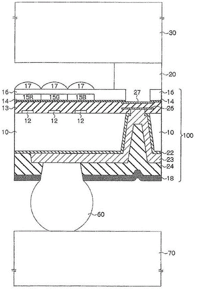
A composition and anti-solder technology, applied in the direction of optical components, photography, electrical components, etc., can solve the problems of insufficient light-shielding properties, insufficient suitability for thick film formation, and inapplicability, and achieve excellent coating uniformity and excellent light-shielding properties Effect

Active Publication Date: 2013-10-02
FUJIFILM CORP
View PDF73 Cites 4 Cited by
  • Summary
  • Abstract
  • Description
  • Claims
  • Application Information

AI Technical Summary

Problems solved by technology

However, since the content of the black colorant contained in this composition will decrease due to the combined use of the black colorant and a colorant other than the black colorant, the light-shielding properties, specifically, the light-shielding properties in the infrared range are insufficient, and Insufficient "thick film forming suitability" makes the composition practically unsuitable

Method used


Image

  • Light-shielding composition, method for producing a light-shielding composition, solder resist, method for forming a pattern, and solid-state imaging device
  • Light-shielding composition, method for producing a light-shielding composition, solder resist, method for forming a pattern, and solid-state imaging device
  • Light-shielding composition, method for producing a light-shielding composition, solder resist, method for forming a pattern, and solid-state imaging device

Examples


preparation example Construction

[0118] Preparation of particle dispersion

[0119] As described above, the light-shielding particles, (B) filler, and (C) filler have been described. It is preferable to disperse each individual particle together with a dispersant, an organic solvent and the like to be described later by mixing and dispersing treatment before producing the light-shielding composition, while using a mill such as a bead mill or Roller Mill) grinds the particles to produce a dispersion of light-shielding particles, a dispersion of (B) filler, and a dispersion of (C) filler. By preparing the respective dispersion liquids before preparing the light-shielding composition, the individual particles can be dispersed into fine particles, and the effect of the present invention can be further achieved.

[0120] The light-shielding dye may not be provided in the form of a dispersion liquid, and may be prepared into a light-shielding composition by dissolving it in an organic solvent or without any treatm...

example 1

[0650] The compositions mentioned below were mixed, and filtered (under the conditions mentioned below), thereby obtaining the light-shielding composition of Example 1.

[0651] (A) Light-shielding particles: 18.5% by mass of YMF-02 (trade name, manufactured by Sumitomo Metal Mining; cesium tungsten oxide (Cs 0.33 WO 3 ), indicating that the particle diameter of the maximum value in the particle diameter distribution is 20 nanometers): 26.97 parts by mass

[0652] (D) Polymerizable compound: A-DCP (trade name, manufactured by Shin-Nakamura Chemical Co., Ltd.; bifunctional polymerizable compound): 5.2 parts by mass

[0653] (E) Photopolymerization initiator: Yanjiagu 907 (trade name, manufactured by BASF Corporation, Japan): 1.24 parts by mass

[0654] Sensitizer: KAYACURE DETX-S (thioxanthone compound, trade name, manufactured by Nippon Kayaku Co., Ltd.): 0.37 parts by mass

[0655] UV absorber: DPO (trade name, manufactured by FUJIFILM Fine Chemicals Co., Ltd.): 0.08 parts...

example 2

[0663] The light-shielding composition of Example 2 was prepared in the same manner as in Example 1, except that the light-shielding particle dispersion used in Example 1 was changed to titanium black dispersion 2.


PUM

PropertyMeasurementUnit
diameteraaaaaaaaaa
diameteraaaaaaaaaa
diameteraaaaaaaaaa

Abstract

The invention provides a light-shielding composition which has suitability for thick film formation, provides a film having an excellent coating uniformity, has thickness uniformity on uneven surface, and has an excellent light-shielding property of light in an infrared region. The light-shielding composition includes: (A) any one of a light-shielding particle or a light-shielding dye; (B) a first filler having a particle diameter of from 100 nm to 3,000 nm, the particle diameter being a maximum value in a particle diameter distribution of the first filler; and (C) a second filler having a particle diameter of from 5 nm to 90 nm, the particle diameter being a maximum value in a particle diameter distribution of the second filler.

Description

technical field [0001] The present invention relates to a light-shielding composition, a method for producing the light-shielding composition, a solder resist formed using the light-shielding composition, a method for forming a pattern, and a solid-state imaging element. Background technique [0002] Solid-state imaging elements used in mobile phones, digital cameras, digital televisions, security cameras, and the like are photoelectric conversion elements integrated into circuits using semiconductor element production technology. According to the recent trend of miniaturization and weight reduction of mobile phones and digital cameras, miniaturization of solid-state imaging components is even more required. [0003] In order to realize miniaturization of solid-state imaging devices, methods of using through electrodes and forming thin-film silicon wafers have been proposed. The miniaturization of solid-state imaging devices can be achieved by forming silicon wafers in the ...

Claims


Application Information

Patent Timeline
Patent Type & Authority Applications(China)
IPC IPC(8): G02B5/22G03F7/004H01L27/14H05K3/28
CPCG02B3/0056G02B5/201G02B5/223G02B7/021H05K1/0274H05K3/3452H01L27/14621H01L27/14623G03F7/0047G03F7/027G03F7/105G03F7/0041
Inventor 室祐继玉田芳纪久保田诚
Owner FUJIFILM CORP
Learn More