


Quick Research
Generate reliable direction feasibility study reports for your R&D in just a few steps.

Technical Q&A
Discover and master advanced knowledge NOW. Basics, ideas, possibilities, all at once.

Find Solutions
As an expert in R&D theories, this can generate solutions to your technical problems instantly.

Evaluate Feasibility
Analyze your overall solution with one click, know your potential R&D risks in advance.

Monitor Landscape
Get weekly tech updates, stay abreast of the latest tech innovations and key insights.
Fixture for sintering semiconductor device and sintering method for plurality of tube cores of semiconductor laser
A technology of semiconductors and lasers, which is applied in the field of semiconductor optoelectronics, can solve the problems of laser stability, lifespan and pass rate adverse effects, chips and heat sinks cannot be uniformly contacted, and batch sintering is not suitable, so as to reduce sintering voids and improve lifespan , quality and reliable effect
- Summary
- Abstract
- Description
- Claims
- Application Information
AI Technical Summary
Problems solved by technology
Method used
Image


Examples
Embodiment 1
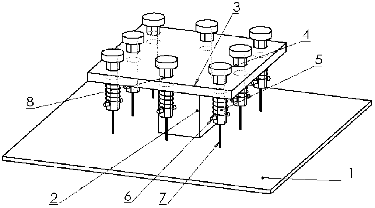
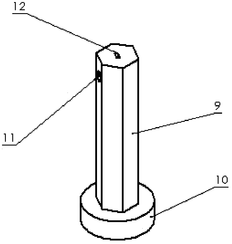
[0035] A sintering jig for a semiconductor device, the structure of which is as follows figure 1 , 2 As shown, it includes a base 1, a support frame 2, a cover plate 3, a lifting column 4, a spring 5, a screw 6, a fixing column 7, a slot 8, a wire hole 11, and a groove 12. The base 1 is a flat plate, and a cuboid support frame 2 is installed in its center, and a rectangular cover plate 3 is fixedly installed on the upper end of the support frame 2. There are 8 hexahedral slots 8 on the cover plate 3, and a lifter is placed in each slot 8. Column 4. The lifting column 4 upper end is a circular column cap 10, and the lower part is a hexahedron cylinder 9, which closely cooperates with the slotted hole 8 and can move up and down, but cannot rotate. There is a groove 12 on the bottom surface of the lower end of the lifting column 4, and the fixing column 7 is inserted in the groove 12. Two thread holes 11 are symmetrically opened on the side of the lower end of the lifting colu...
Embodiment 2
[0041] Embodiment 2, a kind of sintering jig for semiconductor devices, as described in embodiment 1, the difference is that the cover plate 3 is a circular flat plate with a diameter of 8 cm, on which there are 9 hexahedral slots 8, which are evenly distributed along the periphery of the cover plate. distributed. Such as Figure 4 shown.
[0042] The method for sintering multiple tube cores of a semiconductor laser using the jig is as in Example 1, and 9 tube cores can be sintered at one time.
Embodiment 3
[0043] Embodiment 3, a kind of sintering jig for semiconductor devices, as described in Embodiment 1, the difference is that the cover plate 3 is a circular flat plate with a diameter of 11 cm, and there are 19 hexahedral slots 8 in two circles inside and outside. The periphery of the cover plate is evenly distributed, with 9 slots in the inner ring and 10 slots in the outer ring. The slots of the inner and outer rings are misplaced, that is, one inner slot is between two outer slots. Such as Figure 5 shown.
[0044] The method for sintering multiple tube cores of a semiconductor laser using the jig is as in Example 1, and 19 tube cores can be sintered at one time. The difference is that the lifting column of the slot hole in the inner ring of the fixture is raised and lowered to fix 9 dies, and then the lifting column of the slot hole in the outer ring is raised and lowered to fix the 10 dies in the outer ring in turn.
PUM
 Abstract
Description
Claims
Application Information
 - R&D Engineer
- R&D Manager
- IP Professional
- Industry Leading Data Capabilities
- Powerful AI technology
- Patent DNA Extraction
Browse by: Latest US Patents, China's latest patents, Technical Efficacy Thesaurus, Application Domain, Technology Topic, Popular Technical Reports.
© 2024 PatSnap. All rights reserved.Legal|Privacy policy|Modern Slavery Act Transparency Statement|Sitemap|About US| Contact US: help@patsnap.com