
Quadrangular leaf-shaped Cu2O-ZnO composite nano-structural semiconductor material, and preparation method thereof

A composite nanostructure, cu2o-zno technology, applied in semiconductor devices, nanotechnology, nanotechnology, etc., can solve the problem of insufficient carrier migration length, photogenerated electron-hole pairs, high recombination rate, influence heterojunction system sunlight Energy utilization efficiency and other issues, to achieve high efficiency light energy utilization, broad commercial application prospects, and a wide range of applications

Inactive Publication Date: 2013-09-04
EAST CHINA NORMAL UNIV
View PDF2 Cites 15 Cited by
  • Summary
  • Abstract
  • Description
  • Claims
  • Application Information

AI Technical Summary

Problems solved by technology

This will lead to defects such as insufficient carrier migration length and high recombination rate of photogenerated electron-hole pairs, which directly affect the solar energy utilization efficiency of the heterojunction system.

Method used


Image

  • Quadrangular leaf-shaped Cu2O-ZnO composite nano-structural semiconductor material, and preparation method thereof
  • Quadrangular leaf-shaped Cu2O-ZnO composite nano-structural semiconductor material, and preparation method thereof
  • Quadrangular leaf-shaped Cu2O-ZnO composite nano-structural semiconductor material, and preparation method thereof

Examples


Embodiment

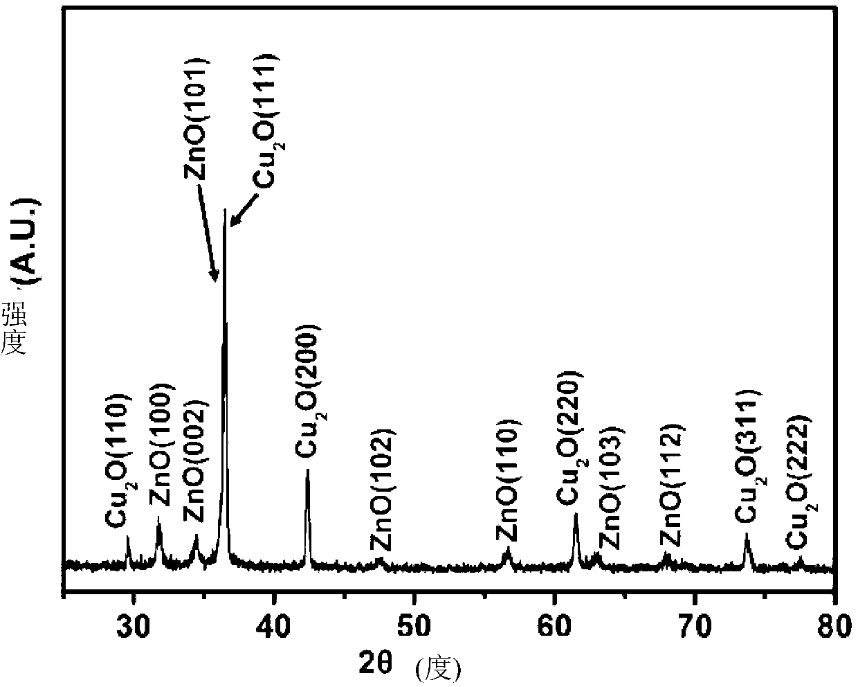
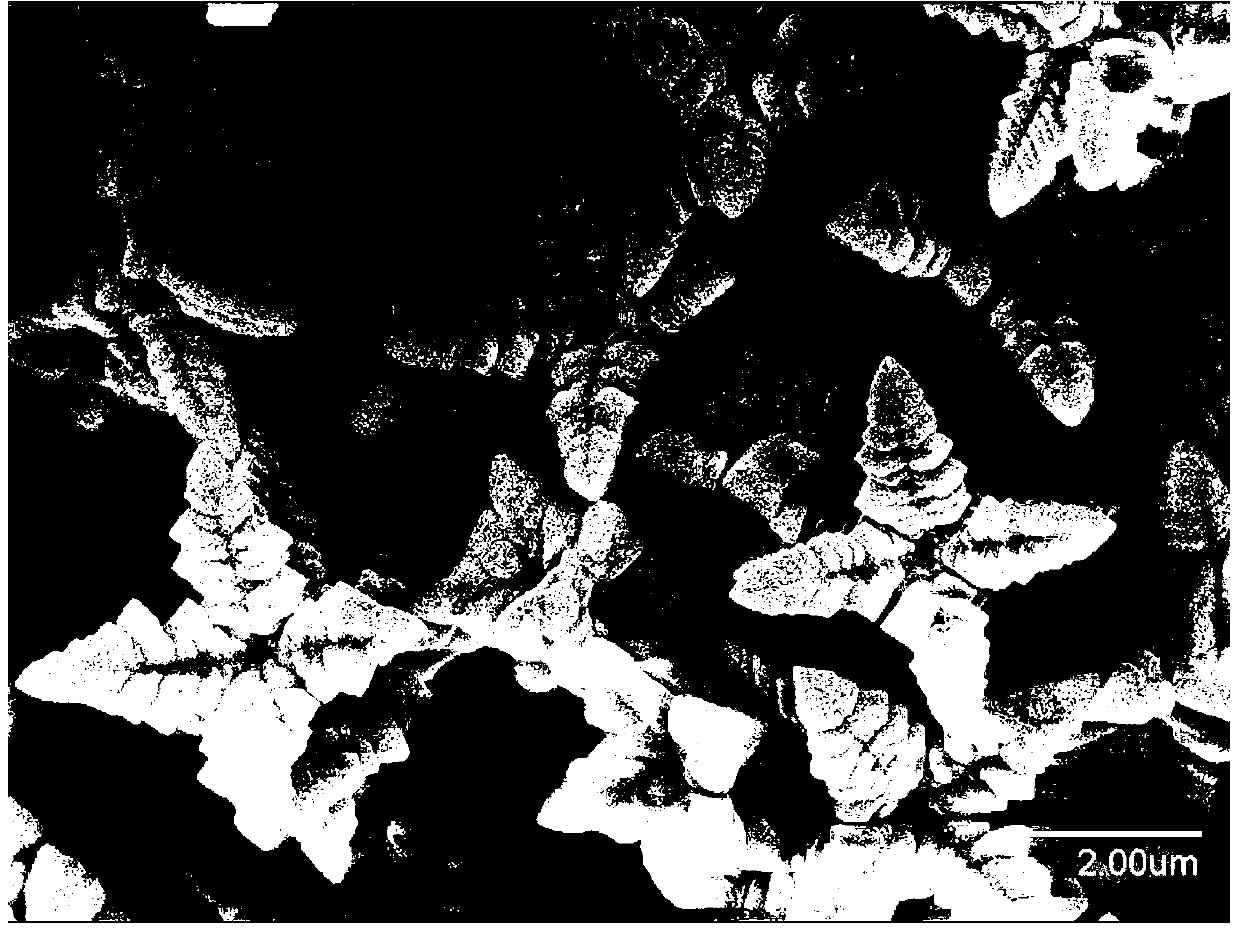
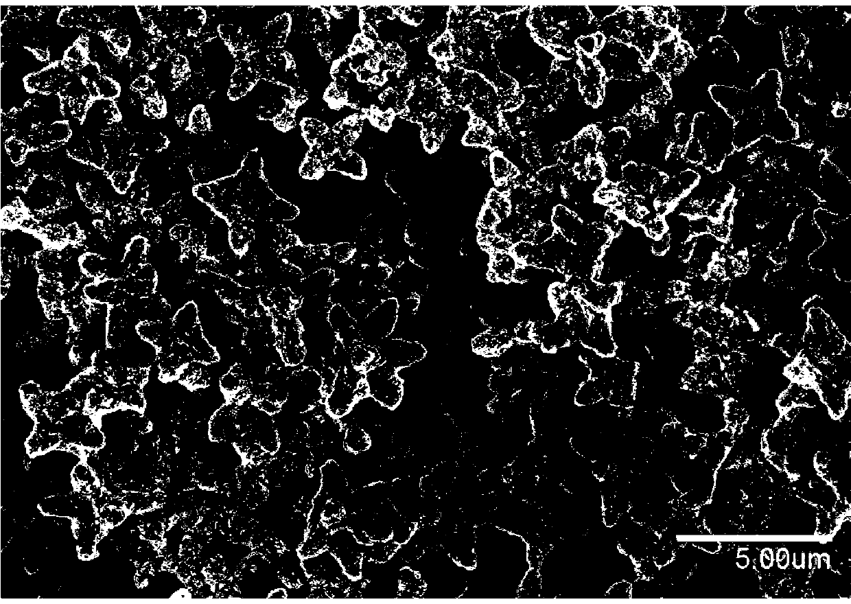
[0029] In this example, the tetragonal leaf-shaped Cu 2 The specific preparation steps of O-ZnO composite nanostructure semiconductor material are as follows:

[0030] 1. Preparation of tetragonal leaf-like Cu 2 O micron particles

[0031] a) Using deionized water as a solvent, prepare 5 mL of copper chloride solution with a concentration of 0.2 mol / L and 5 mL of a solution containing 0.2 g of polyvinylpyrrolidone, dissolve them in 70 mL of deionized water, and stir for 10 minutes with a magnetic stirrer.

[0032] b) Using deionized water as a solvent, prepare 5 mL of potassium carbonate solution with a concentration of 1 mol / L and 5 mL of potassium citrate solution with a concentration of 0.6 mol / L, and pour these two solutions into the solution obtained in the first step. , keep stirring while pouring.

[0033] c) Separately prepare 5 mL of glucose solution with a concentration of 1 mol / L using deionized water as a solvent. When the solution in the second step turns blue, p...


PUM

PropertyMeasurementUnit
sizeaaaaaaaaaa
diameteraaaaaaaaaa
lengthaaaaaaaaaa

Abstract

The invention discloses a quadrangular leaf-shaped Cu2O-ZnO composite nano-structural semiconductor material, comprising a silicon wafer substrate and a quadrangular leaf-shaped Cu2O-ZnO composite nano-structure grown on the silicon wafer substrate, wherein the Cu2O-ZnO composite nano-structure is composed of Cu2O microparticles and ZnO nanoparticles; the Cu2O microparticles have a quadrangular leaf-shaped structure; and the ZnO nanoparticles covers the surface of the Cu2O microparticles. The invention also discloses a preparation method for the quadrangular leaf-shaped Cu2O-ZnO composite nano-structural semiconductor material. The preparation method is simple in operations, and efficiency of light energy utilization of the obtained Cu2O-ZnO hetero nanostructure is significantly increased.

Description

technical field [0001] The invention belongs to the technical field of optoelectronic materials, semiconductor materials and devices, in particular to a quadrangular leaf-shaped Cu 2 Cu with O microparticles and ZnO nanoparticles 2 O-ZnO composite nanostructure semiconductor materials, and stepwise synthesis of Cu 2 O micron particles and ZnO nano particles are prepared by compounding them together. Background technique [0002] Cu 2 O, as a common direct bandgap p-type semiconductor, is widely used in solar cells, hydrogen desorption from water using sunlight, Li-ion batteries, and degradation of organic pollution using visible light, etc. ZnO has the advantages of direct bandgap, wide bandgap (3.3eV, corresponding to near-ultraviolet light at about 380nm), relatively large exciton binding energy (60meV), high carrier mobility, low price, and simple preparation. It is widely used in solar cells, gas sensors, field emission devices and other fields. [0003] Some scient...

Claims


Application Information

Patent Timeline
Patent Type & Authority Applications(China)
IPC IPC(8): C01G3/02C01G9/02B82Y30/00B82Y40/00H01L31/0336
Inventor 汪阳郁可李守川尹海宏宋长青朱自强
Owner EAST CHINA NORMAL UNIV
Learn More