Circuit for capacitive touch applications

A capacitive, circuit technology, applied in electrical components, electronic switches, electrical digital data processing, etc., can solve problems such as spatial nonlinear variation of conversion rate, no low-frequency noise cancellation, surface area and power consumption, etc., to reduce The effect of total surface area and power consumption

Active Publication Date: 2013-08-21
ADVANCED SILICON
View PDF14 Cites 27 Cited by
  • Summary
  • Abstract
  • Description
  • Claims
  • Application Information

AI Technical Summary

Problems solved by technology

Problems in touch panels that include a large number of sensing capacitors are the required surface area and power consumption
The ADC shared by four channels limits the conversion rate and worsens the spatial nonlinearity, that is, the nonlinearity related to the difference between adjacent channels
Since one ADC is used for N channels, its conversion rate is lower compared to other solutions
Also, no low frequency noise cancellation is done in this case

Method used


Image

  • Circuit for capacitive touch applications
  • Circuit for capacitive touch applications
  • Circuit for capacitive touch applications

Examples


Embodiment Construction

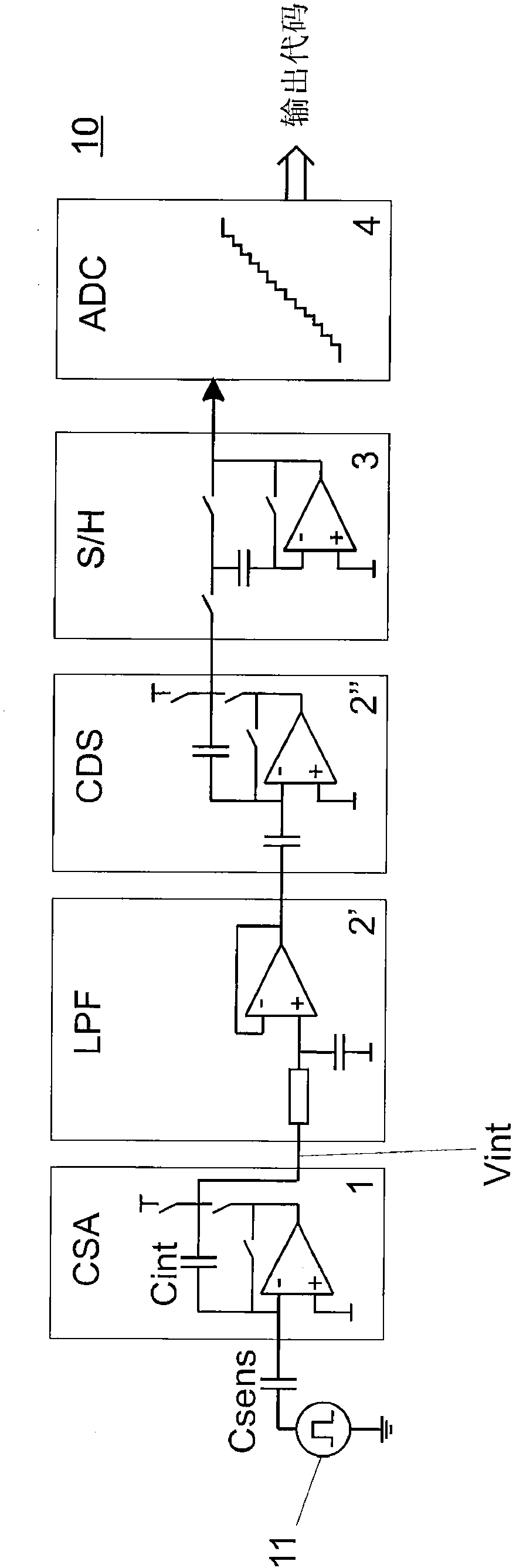
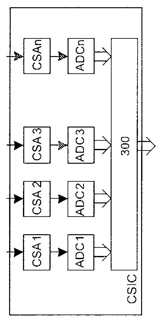
[0065] A capacitive touch device, such as a touch panel, includes an array of sensing capacitors. If an object with good dielectric properties, such as a finger, is approaching the touchpad, the capacitance value of these capacitors will change. The entire array is read by a capacitive sensor integrated circuit (CSIC) at moderate speeds, typically 100-1000fps.

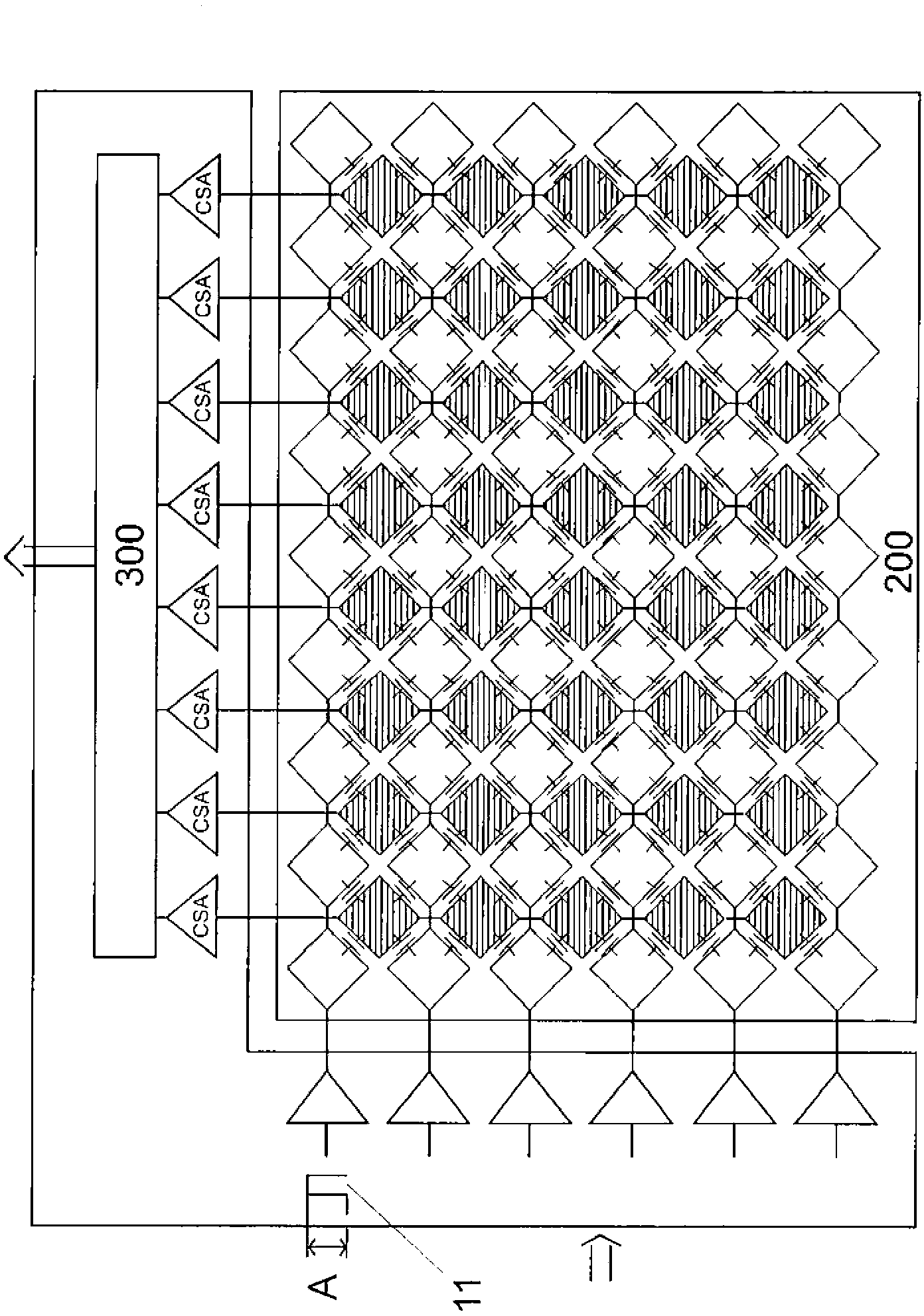
[0066] figure 2 A view of a capacitive touch device with a CSIC is shown. It includes a first number N of rows of sensing capacitors and a second number M of columns of sensing capacitors. The sensing capacitors are all arranged in a matrix, similar to pixels in an image. In one embodiment, N and M may be the same, ie N=M. In other words, the capacitive touch device includes a capacitive sensor array 200 whose dimension is N*M.

[0067] A voltage 11 of amplitude A is applied as the input signal through the sensing capacitors of each row. In a possible operation scheme, each row is sequentially addressed by the i...


PUM


Abstract

A circuit for capacitive touch applications comprising: a charge integrator; a low pass-filter; a correlated double sampler comprising an input capacitor; a sampler and holder; an analog to digital converter. Said low pass-filter having cut-off frequency lower than the Nyquist frequency of the sampler and holder. Said low pass filter comprising said input capacitor and a serial resistor.

Description

technical field [0001] The present invention relates to circuits with digital outputs typically used in capacitive touch applications. Background technique [0002] Capacitive sensors are used in a variety of applications involving object presence detection such as but not limited to touchpads, touch panels, touch screens or projected capacitive displays. [0003] figure 1 A possible capacitive detection measurement circuit 10 is described. Each sensing capacitor C sens is connected to the input of the first block 1 - charge integrator - of the acquisition chain 10 . Since the non-inverting input of the charge integrating amplifier is held at a constant voltage, there is a virtual ground at the inverting input of the amplifier, that is, the input voltage of the charge integrating amplifier is kept constant. Charge sensing against virtual ground allows immunity to power supply noise. The reset phase forces the output voltage of charge integrator 1 V int reached the pred...

Claims


Application Information

Patent Timeline
Patent Type & Authority Applications(China)
IPC IPC(8): H03K17/945
CPCG06F3/04166G06F3/0446H03K17/9622H03K2217/960735H03M1/123H03M1/145H03M1/162H03M1/168H03M1/468G06F3/0416G06F3/044G06F2203/04107
Inventor 侯赛因·巴兰奥利维尔·NYS诺曼·沙帕特弗朗索瓦·瓦登斯
Owner ADVANCED SILICON
Why Eureka
Try Eureka