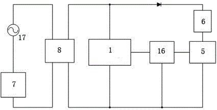
A dimmable led lighting drive circuit
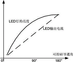
A technology of LED lighting and driving circuit, which is applied in the direction of lighting devices, lamp circuit layout, light source, etc. It can solve the problems of slow dimming response speed, unnatural dimming process, and delay of LED light brightness, so as to improve the dimming response Speed and dimming accuracy, simple structure, easy to integrate effects
- Summary
- Abstract
- Description
- Claims
- Application Information
AI Technical Summary
Problems solved by technology
Method used
Image
Examples
Embodiment 1
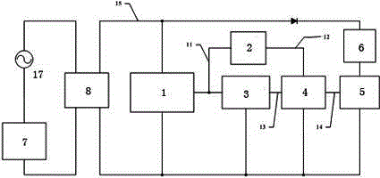
[0024] Such as Figure 5 As shown, the signal 11 passes through the delay module and the logic control module. When the signal 11 is at a low level (within the SCR control angle), the switch S1 is turned off, S2 is turned on, the capacitor C1 is discharged through the resistor R1, and the voltage on the capacitor C1 Signal 13 is an exponential curve. The pulse generator 2 generates a pulse signal 12 at the rising edge of the signal 11 (the moment when the thyristor is turned on), and the signal 12 is input to the control terminal of the sample and hold module 4, and the sample and hold module 4 responds to the signal 13 when each pulse signal comes. Sample and hold. Image 6 It is a relationship diagram of the output signal 11 of the phase detection module 1, the output signal 13 of the LOG curve generator 3, and the control signal of the sample and hold module 2. When the thyristor dimmer controls the phase change, the discharge time of capacitor C1 and the rising edge mome...
Embodiment approach 2
[0026] Such as Figure 8 As shown, the signal 11 passes through the delay module and the logic control module. When the signal 11 is at a low level (within the SCR control angle), the switch S1 is turned on, and the S2 is turned off. The power supply charges the capacitor C1 through the resistor R1, and the capacitor C1 The voltage signal 13 is an exponential curve. The pulse generator 2 generates a pulse signal 12 at the rising edge of the signal 11 (that is, the moment when the thyristor is turned on), and the signal 12 is input to the control terminal of the sampling and holding module 4, and the sampling and holding module 4 performs the signal processing when each pulse signal comes. 13 Sample and hold. Figure 9It is a relationship diagram of the output signal 11 of the phase detection module 1, the output signal 13 of the LOG curve generator 3, and the control signal of the sample and hold module 2. When the thyristor dimmer controls the phase change, the rising edge ...
PUM
 Abstract
Description
Claims
Application Information
 - R&D
- Intellectual Property
- Life Sciences
- Materials
- Tech Scout
- Unparalleled Data Quality
- Higher Quality Content
- 60% Fewer Hallucinations
Browse by: Latest US Patents, China's latest patents, Technical Efficacy Thesaurus, Application Domain, Technology Topic, Popular Technical Reports.
© 2025 PatSnap. All rights reserved.Legal|Privacy policy|Modern Slavery Act Transparency Statement|Sitemap|About US| Contact US: help@patsnap.com


