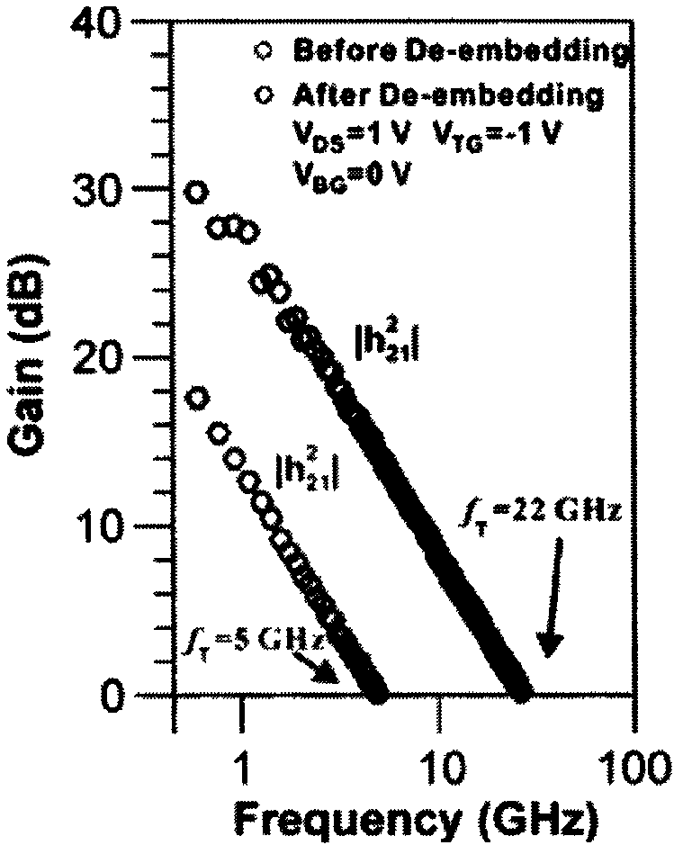
Grapheme field effect transistor and preparation method thereof

A field-effect transistor, graphene technology, applied in semiconductor/solid-state device manufacturing, semiconductor devices, electrical components, etc., can solve the problems of non-uniform distribution of two-dimensional electron gas, destruction of electrical neutrality, doping effect, etc.

Inactive Publication Date: 2013-08-21
XIDIAN UNIV
View PDF1 Cites 15 Cited by
  • Summary
  • Abstract
  • Description
  • Claims
  • Application Information

AI Technical Summary

Problems solved by technology

At the same time, these interface states, impurities and dangling bonds will lead to non-uniform distribution of two-dimensional electron gas and doping effects in the graphene film near the Dirac point, thereby destroying the electrical neutrality near the Dirac point.

Method used


Image

  • Grapheme field effect transistor and preparation method thereof
  • Grapheme field effect transistor and preparation method thereof
  • Grapheme field effect transistor and preparation method thereof

Examples


Embodiment Construction

[0027] In order to make the technical means, creative features, objectives and effects achieved by the present invention easy to understand, the present invention will be further described below in conjunction with specific embodiments.

[0028] Such as figure 1 As shown, a graphene field effect transistor comprises a substrate 110, a graphene channel layer 130, a bottom gate dielectric layer 120, a top gate dielectric layer 140, a source electrode 150, a drain electrode 160 and a top gate electrode 170, and the top gate The dielectric layer 140 and the bottom gate dielectric layer 120 are respectively located above and below the graphene channel layer 130, the substrate 110 is located below the bottom gate dielectric layer 120, and the source electrode 150 and the drain electrode 160 are respectively located on both sides of the graphene channel layer. end, the top gate electrode 170 is located on the top gate dielectric layer 140 . Wherein, the material constituting the top...


PUM


Abstract

The invention provides a grapheme field effect transistor and a preparation method of the grapheme field effect transistor. According to the grapheme field effect transistor, h-BN is used as gate media and used for replacing oxides such as SiO2 and HfO2 in an existing grapheme field effect transistor, and therefore performance of the grapheme field effect transistor is improved. Due to the fact that energy of a surface optic phonon mode of the h-BN is two times larger than that of a similar mode of SiO2, characteristics of the grapheme field effect transistor with the h-BN as the gate media under high frequency and a strong electric field are better than characteristics of a typical grapheme field effect transistor with the SiO2 as the gate media.

Description

technical field [0001] The invention relates to the technical field of field effect transistors, in particular to a graphene field effect transistor and a preparation method thereof. Background technique [0002] Using SiO 2 As a gate dielectric, the performance of the graphene channel film is far inferior to that of its intrinsic state. However, the performance of the graphene trench field effect device with a suspended structure has been significantly improved. However, the suspended structure severely restricts the structure and functionality of the device, making it impossible for practical application. [0003] Achieving substrate-supported geometries close to the quality of suspended graphene samples is an important research direction for future graphene device structures. Transport properties of graphene films mechanically exfoliated and transferred onto single-crystal h-BN substrates at different temperatures and magnetic fields, with Compared with graphene-based...

Claims


Application Information

Patent Timeline
Patent Type & Authority Applications(China)
IPC IPC(8): H01L29/78H01L29/423H01L21/336
Inventor 马中发庄弈琪吴勇张鹏张策包军林
Owner XIDIAN UNIV
Why Eureka
Try Eureka