Pixel circuit and driving method thereof
A pixel circuit and circuit technology, applied in static indicators, instruments, etc., can solve problems such as uneven film thickness and non-uniform electrical performance of light-emitting devices, and achieve the goal of eliminating uneven film thickness, improving quality, and improving compensation effects Effect
- Summary
- Abstract
- Description
- Claims
- Application Information
AI Technical Summary
Problems solved by technology
Method used
Image
Examples
Embodiment 1
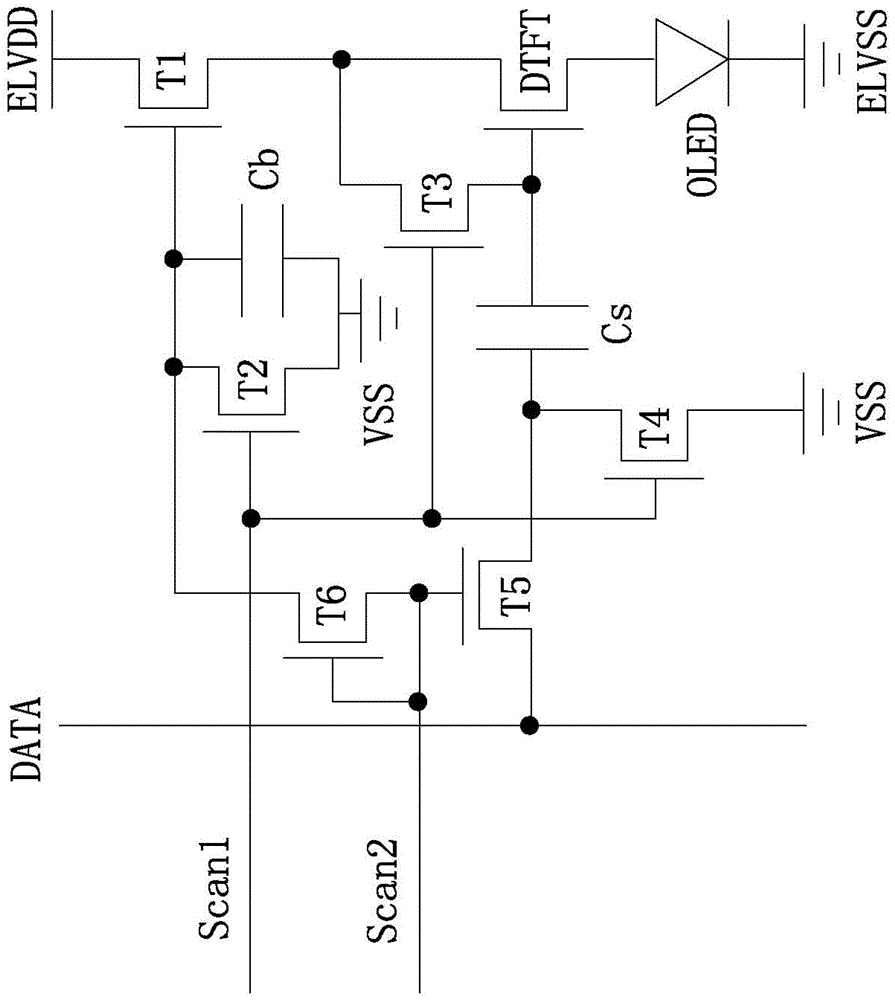
[0042] see figure 1 As shown, the pixel circuit described in the embodiment of the present invention is mainly used for the driving compensation of each light-emitting device in the active matrix light-emitting organic electric display tube. Each light-emitting device is driven and compensated by a pixel circuit, and each pixel circuit includes: Subcircuits, charging subcircuits, driving subcircuits and light emitting devices; wherein,
[0043] The first terminal of the light emitting device OLED is connected to the second voltage terminal ELVSS;
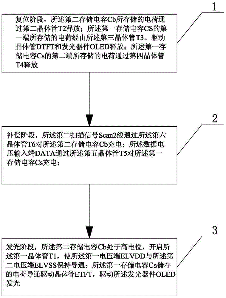
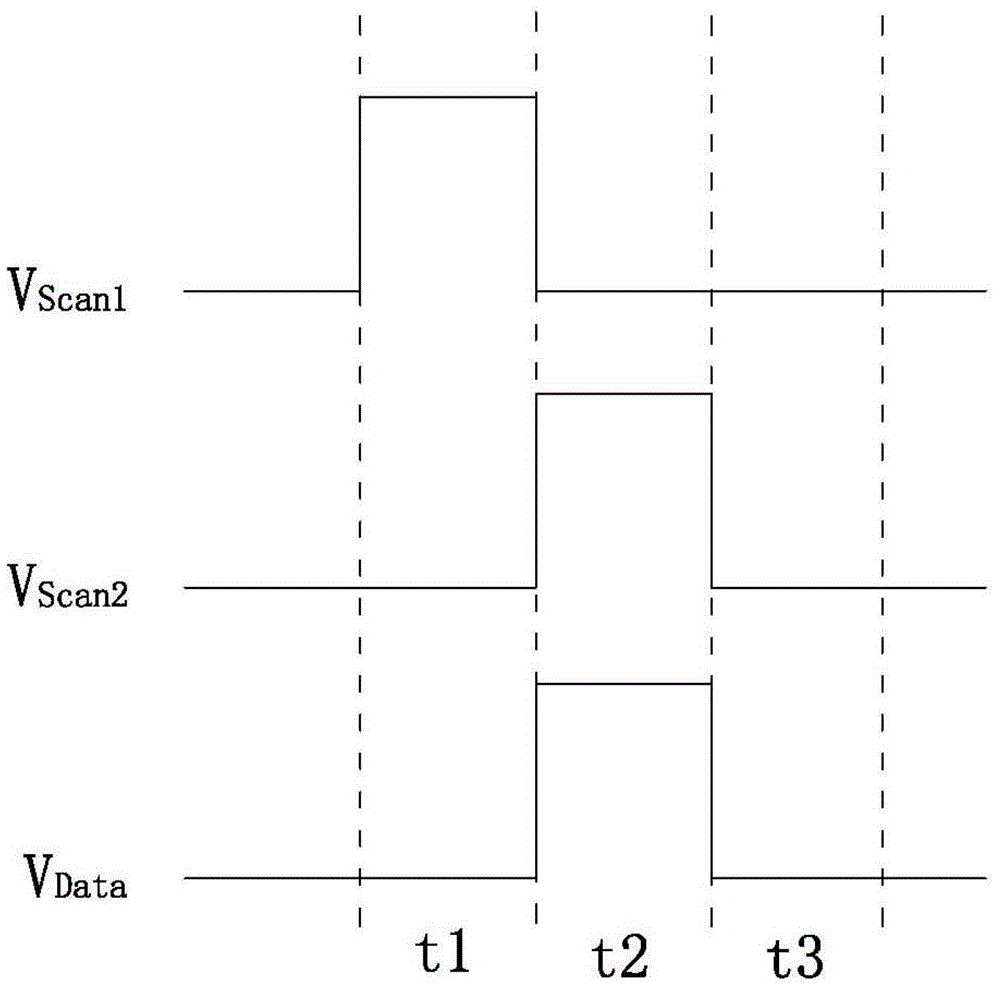
[0044] The driving sub-circuit includes a driving transistor DTFT, a first transistor T1, a third transistor T3, a first storage capacitor Cs, and a second storage capacitor Cb, and the source of the driving transistor DTFT is connected to the drain of the first transistor T1 and the drain of the third transistor T3, the drain of the driving transistor DTFT is connected to the second terminal of the light emitting device OLED, the ...
Embodiment 2
[0067] The pixel circuit and driving method in this embodiment are improvements on the basis of Embodiment 1. The technical content disclosed in Embodiment 1 will not be described repeatedly, and the content disclosed in Embodiment 1 also belongs to the content disclosed in this embodiment.
[0068] see Figure 4 As shown, as a modified technical solution of the technical solution in Embodiment 1; the pixel circuit also includes a third scanning signal line Scan3; specifically: the charging sub-circuit includes a fifth transistor T5 and a sixth transistor T6, so The source of the fifth transistor T5 is connected to the data voltage input terminal DATA, the drain of the fifth transistor T5 is connected to the source of the fourth transistor T4, and the gate of the fifth transistor T5 is connected to the second scanning signal line Scan2; the gate of the sixth transistor T6 and the source of the sixth transistor T6 are connected to the third scanning signal line Scan3, and the d...
PUM
 Abstract
Description
Claims
Application Information
 - R&D Engineer
- R&D Manager
- IP Professional
- Industry Leading Data Capabilities
- Powerful AI technology
- Patent DNA Extraction
Browse by: Latest US Patents, China's latest patents, Technical Efficacy Thesaurus, Application Domain, Technology Topic, Popular Technical Reports.
© 2024 PatSnap. All rights reserved.Legal|Privacy policy|Modern Slavery Act Transparency Statement|Sitemap|About US| Contact US: help@patsnap.com


