Probe unit structure and manufacturing method thereof

The technology of a probe unit and manufacturing method, which is applied in the field of probe structure, can solve the problems of damage to the contact probe 40, difficulty in manufacturing and assembling, and narrow spacing, and achieve the effects of simplicity, convenience, cost, easy assembly, and improved use stability

Active Publication Date: 2013-08-14
CERTAIN MICRO APPL TECH
View PDF9 Cites 1 Cited by
  • Summary
  • Abstract
  • Description
  • Claims
  • Application Information

AI Technical Summary

Problems solved by technology

[0004] However, in recent years, semiconductor integrated circuits have made remarkable progress in high integration and miniaturization. As far as the probe unit is concerned, in order to match the progress of this technology, the diameter of each contact probe will also be reduced. The distance between each contact probe is narrowed; however, the smaller the diameter of the above-mentioned contact probe 40, the smaller the upper hole groove 101 and the lower hole groove 201, so that the upper hole groove 101 and the lower hole groove 201 are smaller and smaller. There is a slight error in the alignment between them, which leads to the fact that the contact probe 40 is positioned on the upper positioning substrate 10, but cannot be positioned on the lower positioning substrate 20. At this time, forced assembly will damage the contact probe 40; therefore, contact When the diameter of the probe 40 shrinks, the existing probe unit has great difficulties in making and assembling and cannot break through

Method used


Image

  • Probe unit structure and manufacturing method thereof
  • Probe unit structure and manufacturing method thereof
  • Probe unit structure and manufacturing method thereof

Examples


Embodiment Construction

[0082] The detailed description and technical content of the present invention will be described as follows with the accompanying drawings, but the attached drawings are only for illustration purposes and are not intended to limit the present invention.

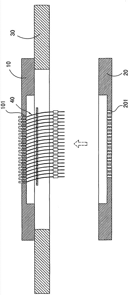
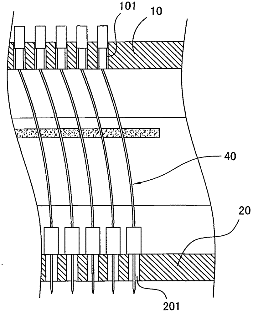
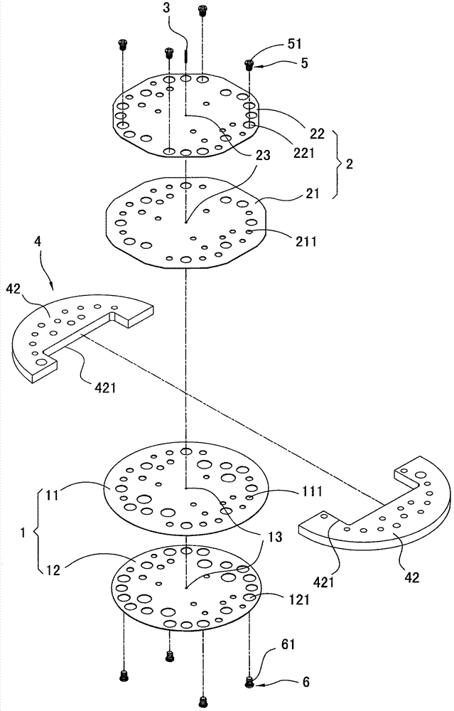
[0083] Please refer to Figure 3 to Figure 6 As shown, the present invention provides a probe unit structure and a manufacturing method thereof. The probe unit structure mainly includes a first positioning substrate 1 , a second positioning substrate 2 , a plurality of contact probes 3 and a spacer 4 .

[0084] The first positioning substrate 1 includes a first inner insulating plate 11 and a first outer insulating plate 12 bonded to the first inner insulating plate 11, the first inner insulating plate 11 and the first outer insulating plate 12 are jointly provided with a plurality of The first pin hole 13 ; moreover, the first inner insulating plate 11 is provided with a plurality of locking holes 111 , and the first outer i...


PUM


Abstract

The invention discloses a probe unit structure and a manufacturing method thereof. The probe unit structure comprises a first positioning base plate, a second positioning base plate, contact probes and a space piece, wherein first needle threading holes are formed in the first positioning base plate; second needle threading holes are formed in the second positioning base plate; the first positioning base plate and the second positioning base plate are mutually overlaid when assembled; a gap is formed between the first positioning base plate and the second positioning base plate through a lifting tool; the contact probe penetrates through the first needle threading holes and the second needle threading holes; an accommodating chamber for accommodating the contact probes is formed in the space piece through the gap; the first positioning base plate slides relative to the second positioning base plate, so that the first needle threading holes and the second needle threading holes produce deviation, and two ends of the contact probe are clamped and positioned by the first positioning base plate and the second positioning base plate respectively. Accordingly, the thinning of the contact probes can still facilitate the manufacturing of a probe unit.

Description

technical field [0001] The invention relates to a probe structure for detection, in particular to a probe unit structure and a manufacturing method thereof. Background technique [0002] When manufacturing semiconductor integrated circuits such as IC chips, electrical characteristics are inspected to detect defective products; specifically, when inspecting semiconductor integrated circuits or liquid crystal panels, etc., it is possible to know the characteristics of the semiconductor integrated circuits to be inspected. Whether there is an electrical short circuit or disconnection in the wiring pattern; at the same time, in order to seek electrical connection between the inspection object and the signal processing device that outputs the inspection signal, a probe unit that accommodates multiple conductive contact probes will be used, To be electrically connected to the inspection object and the signal processing device respectively. [0003] Traditional probe units such as...

Claims


Application Information

Patent Timeline
IPC IPC(8): G01R1/073G01R1/04
Inventor 何震宏叶威男
Owner CERTAIN MICRO APPL TECH
Why Eureka
Try Eureka