Display panel and preparation method thereof, mask plate the preparation method thereof, and display device
A technology for a display panel and a display substrate, which is applied in the fields of display devices, mask plates and their preparations, display panels and their preparations, can solve problems such as poor stability of supporting array substrates and reduce product performance, and achieves improved exposure intensity and improved product performance. performance, the effect of increasing stability
- Summary
- Abstract
- Description
- Claims
- Application Information
AI Technical Summary
Problems solved by technology
Method used
Image
Examples
Embodiment 1
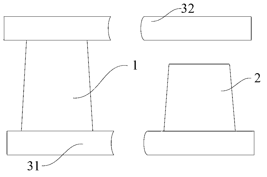
[0047] like Figure 2a and Figure 2b As shown, the display panel provided in this embodiment includes a first display substrate 31 and a second display substrate 32 disposed opposite to each other, and a main spacer 1 and an auxiliary spacer 1 disposed between the first display substrate 31 and the second display substrate 32 The spacer 2, the main spacer 1 and the auxiliary spacer 2 are all arranged on the first display substrate 31, or both the main spacer 1 and the auxiliary spacer 2 are arranged on the second display substrate 32, and at least The end face of the suspended end of an auxiliary spacer 2 is a plane, such as Figure 2a shown, and / or the end face of the suspended end of at least one auxiliary spacer 2 is convex, such as Figure 2b shown.
[0048]In the display panel provided by the present invention, the main spacer 1 and the auxiliary spacer 2 are arranged on the same display substrate, and the end face of the suspended end of at least one auxiliary spacer...
Embodiment 2
[0054] like image 3 As shown, the present embodiment provides a halftone mask for preparing a display panel, comprising a base substrate 4 and a light-shielding film layer 5 located on the base substrate 4, the light-shielding film layer 5 having an auxiliary spacer and an auxiliary spacer 2 One-to-one corresponding halftone light transmission area D, the halftone light transmission area D is as follows image 3 As shown by the dotted line box, the halftone light-transmitting area D is provided with a half-tone light-transmitting film 7, and the central area of at least one half-tone light-transmitting film 7 is a hollow area.
[0055] When using the halftone mask provided by the present invention to prepare the auxiliary spacer in the display panel, the central area of the halftone light-transmitting area D is a hollow area. The phenomenon of light interference in the area, so as to fully expose the center position of the end face of the suspended end of the auxiliary s...
Embodiment 3
[0058] like Figure 4 As shown, this embodiment provides a method for preparing a halftone mask, including:
[0059] Step S401 : forming a light-shielding film layer on a base substrate, and forming an opening area of a halftone light-transmitting region on the light-shielding film layer through a patterning process;
[0060] Step S402 : forming a halftone light-transmitting film on the base substrate after the above steps have been completed, and forming a hollow region in the central region of the halftone light-transmitting region through a patterning process.
[0061] In a specific implementation manner, step S401 may specifically include:
[0062] A light-shielding film layer 5 is formed on the base substrate 4, and a layer of photoresist 6 is coated on the light-shielding film layer 5, such as Figure 5a shown;
[0063] Using a drawing and developing process, the photoresist is formed into a photoresist removal area and a photoresist retention area; the photoresist ...
PUM
 Abstract
Description
Claims
Application Information
 - R&D Engineer
- R&D Manager
- IP Professional
- Industry Leading Data Capabilities
- Powerful AI technology
- Patent DNA Extraction
Browse by: Latest US Patents, China's latest patents, Technical Efficacy Thesaurus, Application Domain, Technology Topic, Popular Technical Reports.
© 2024 PatSnap. All rights reserved.Legal|Privacy policy|Modern Slavery Act Transparency Statement|Sitemap|About US| Contact US: help@patsnap.com


