Thyristor gate-cathode junction and method for preparing gate-commutated thyristor with the structure
A technology of gate commutation and thyristor, which is applied in semiconductor/solid-state device manufacturing, electrical components, circuits, etc., and can solve problems such as high doping concentration
- Summary
- Abstract
- Description
- Claims
- Application Information
AI Technical Summary
Problems solved by technology
Method used
Image
Examples
Embodiment 1
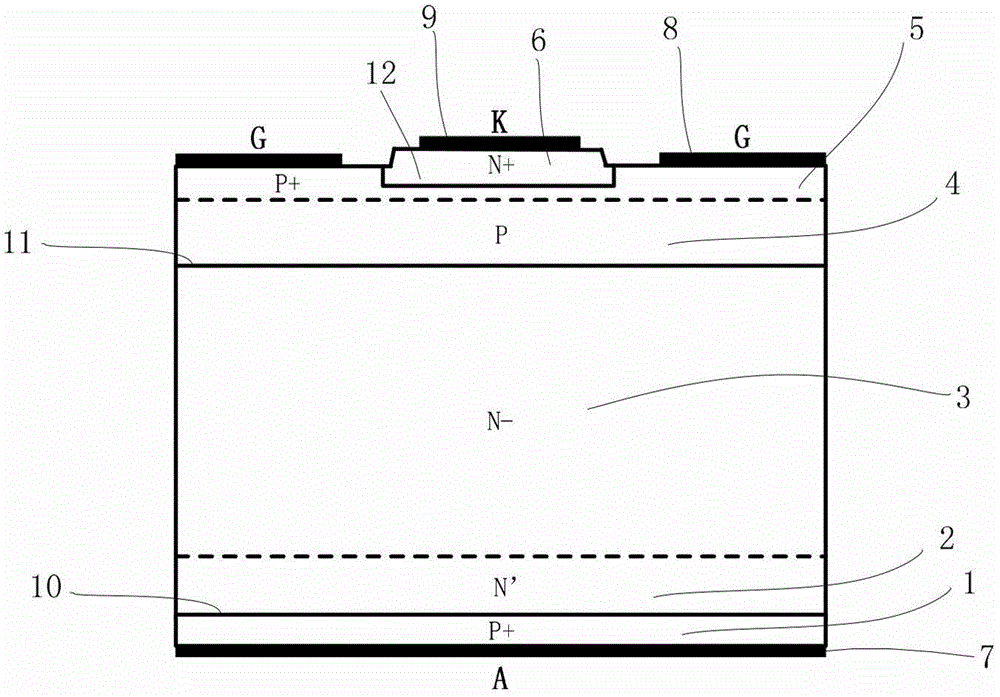
[0204] as attached Figure 43 A specific implementation method of a gate-commutated thyristor manufacturing method shown in the process of A. The gate-commutated thyristor includes more than one cell, and the manufacturing method of the gate-commutated thyristor includes more than one gate-commutated thyristor cell. The preparation method, wherein, the preparation method of a single gate commutated thyristor cell comprises the following steps:
[0205] S101: Prepare N-type substrate, as attached Figure 22 shown;
[0206] S102: Perform selective P+ diffusion treatment on the front side of the N-type substrate to form a P+ short base region 5, as shown in the attached Figure 23 As shown in the figure, the width L between the two P+ short base regions 5 is adjustable;
[0207] S103: Perform P diffusion treatment on the front side of the N-type substrate to form the P base region 4, and form the J2 junction 11 between the P base region 4 and the N-substrate 3, as shown in the...
Embodiment 2
[0218] as attached Figure 43 A specific implementation of a gate commutated thyristor manufacturing method shown in the process of C, the gate commutated thyristor includes more than one cell, the gate commutated thyristor preparation method includes more than one gate commutated thyristor cell The preparation method, the preparation method of a single gate commutated thyristor cell comprises the following steps:
[0219] S301: preparing an N-type substrate;
[0220] S302: Perform P diffusion treatment on the front side of the N-type substrate to form a P base region 4, and form a J2 junction 11 between the P base region 4 and the N-substrate 3;
[0221] S303: performing selective P+ diffusion treatment on the front side of the N-type substrate to form a P+ short base region 5;
[0222] S304: performing N' diffusion treatment on the back surface of the N-type substrate to form an N' buffer layer 2;
[0223]S305: performing N+ pre-deposition treatment on the front side of t...
Embodiment 3
[0234] as attached Figure 43 A specific implementation method of a gate-commutated thyristor manufacturing method shown in the process of B, the gate-commutated thyristor includes more than one cell, and the manufacturing method of the gate-commutated thyristor includes more than one gate-commutated thyristor cell The preparation method, the preparation method of a single gate commutated thyristor cell comprises the following steps:
[0235] S201: Prepare N-type substrate, as attached Figure 32 shown;
[0236] S202: Perform P' diffusion treatment on the front side of the N-type substrate, as shown in the attached Figure 33 shown;
[0237] S203: Perform selective P+ diffusion treatment on the front side of the N-type substrate to form a P+ short base region 5, as shown in the attached Figure 34 shown;
[0238] S204: Perform P diffusion treatment on the front side of the N-type substrate to form the P base region 4, and form the J2 junction 11 between the P base region ...
PUM
 Abstract
Description
Claims
Application Information
 - R&D
- Intellectual Property
- Life Sciences
- Materials
- Tech Scout
- Unparalleled Data Quality
- Higher Quality Content
- 60% Fewer Hallucinations
Browse by: Latest US Patents, China's latest patents, Technical Efficacy Thesaurus, Application Domain, Technology Topic, Popular Technical Reports.
© 2025 PatSnap. All rights reserved.Legal|Privacy policy|Modern Slavery Act Transparency Statement|Sitemap|About US| Contact US: help@patsnap.com


