Nonvolatile memory element and manufacturing method thereof
A technology of non-volatile storage and components, which is applied to electrical components, semiconductor devices, electric solid-state devices, etc., and can solve problems such as misoperation and instability of non-volatile storage components
- Summary
- Abstract
- Description
- Claims
- Application Information
AI Technical Summary
Problems solved by technology
Method used
Image
Examples
Embodiment approach 1
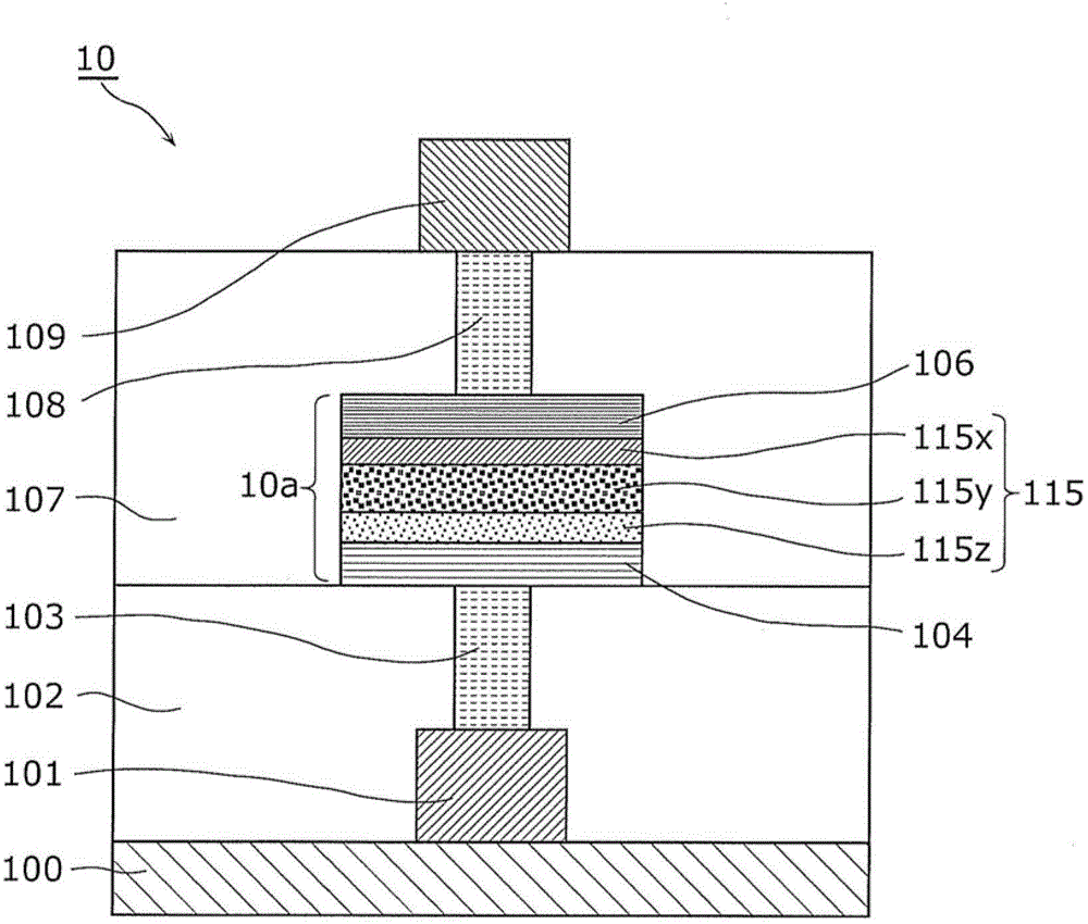
[0105] figure 1 It is a cross-sectional view showing a configuration example of the resistance variable nonvolatile memory element 10 according to Embodiment 1 of the present invention. like figure 1 As shown, the variable resistance nonvolatile memory element 10 of Embodiment 1 has a substrate 100 on which a first wiring 101 is formed, a first interlayer insulating layer 102, and a first contact plug 103 (50 to 300 nm in diameter). ), wherein the first interlayer insulating layer 102 is composed of a silicon oxide film (film thickness 300-500 nm) formed on the substrate 100 covering the first wiring 101; the first contact plug 103 mainly contains tungsten , formed through the first interlayer insulating layer 102 and electrically connected to the first wiring 101 . Then, on the first interlayer insulating layer 102, the variable resistance element 10a having the second electrode (lower electrode in this embodiment) 104 (film 5 to 100 nm in thickness), the variable resist...
Embodiment approach 2
[0134] Image 6 It is a cross-sectional view showing a configuration example of the resistance variable nonvolatile memory element 20 according to Embodiment 2 of the present invention. and figure 1 The shown variable resistance nonvolatile memory element 10 according to Embodiment 1 of the present invention is different in that each layer of the variable resistance layer and the first electrode and the second electrode are arranged upside down. That is, in contrast to the arrangement of the first electrode 106 above the second electrode 104 in Embodiment 1, the first electrode 106 is arranged below the second electrode 104 in this embodiment.
[0135] like Image 6 As shown, the variable resistance layer 125 of the variable resistance nonvolatile memory element 20 of Embodiment 2 is also made of the first transition metal oxide layer 125x, the second transition metal oxide layer 125y, and the third transition metal oxide layer. layer 125z is a stacked structure consisting...
Embodiment approach 3
[0148] Figure 8 It is a cross-sectional view showing a structural example of the resistance variable nonvolatile memory element 30 according to Embodiment 3 of the present invention. and figure 1 The shown variable resistance nonvolatile memory element 10 according to Embodiment 1 of the present invention has the same structural elements, but the film thickness and resistivity of each variable resistance layer are different.
[0149] That is, in the nonvolatile memory element 10 of Embodiment 1, tantalum oxide is used as the first to third transition metal oxide layers. In this case, the structure is: TaO as the third transition metal oxide layer 115z z The oxygen content rate z=0.68 (resistivity: 0.33mΩcm), the film thickness is 10nm, as the TaO of the second transition metal oxide layer 115y y The oxygen content rate z=1.29 (resistivity: 6mΩcm), the film thickness is 35nm, as the TaO of the first transition metal oxide layer 115x x The oxygen content rate x=2.4 (resisti...
PUM
| Property | Measurement | Unit |
|---|---|---|
| thickness | aaaaa | aaaaa |
| thickness | aaaaa | aaaaa |
| thickness | aaaaa | aaaaa |
Abstract
Description
Claims
Application Information
 - R&D
- Intellectual Property
- Life Sciences
- Materials
- Tech Scout
- Unparalleled Data Quality
- Higher Quality Content
- 60% Fewer Hallucinations
Browse by: Latest US Patents, China's latest patents, Technical Efficacy Thesaurus, Application Domain, Technology Topic, Popular Technical Reports.
© 2025 PatSnap. All rights reserved.Legal|Privacy policy|Modern Slavery Act Transparency Statement|Sitemap|About US| Contact US: help@patsnap.com


