A kind of semiconductor device and its manufacturing method

A manufacturing method and semiconductor technology, applied in semiconductor/solid-state device manufacturing, transistors, electrical components, etc., can solve problems such as point defects, Mo metal short circuits, line defects, etc., so as to reduce the manufacturing cycle, simplify the process flow, and avoid adverse factors. Effect

Active Publication Date: 2016-04-13
NANJING CEC PANDA LCD TECH
View PDF3 Cites 0 Cited by
  • Summary
  • Abstract
  • Description
  • Claims
  • Application Information

AI Technical Summary

Problems solved by technology

If the remaining Ti metal causes a short circuit of the Mo metal on both sides, it will cause a point defect or a line defect.

Method used


Image

  • A kind of semiconductor device and its manufacturing method
  • A kind of semiconductor device and its manufacturing method
  • A kind of semiconductor device and its manufacturing method

Examples


Embodiment Construction

[0029] Below in conjunction with accompanying drawing and specific embodiment, further illustrate the present invention, should be understood that these embodiments are only for illustrating the present invention and are not intended to limit the scope of the present invention, after having read the present invention, those skilled in the art will understand various aspects of the present invention Modifications in equivalent forms all fall within the scope defined by the appended claims of this application.

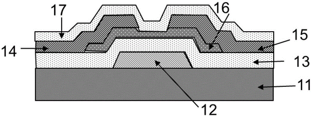
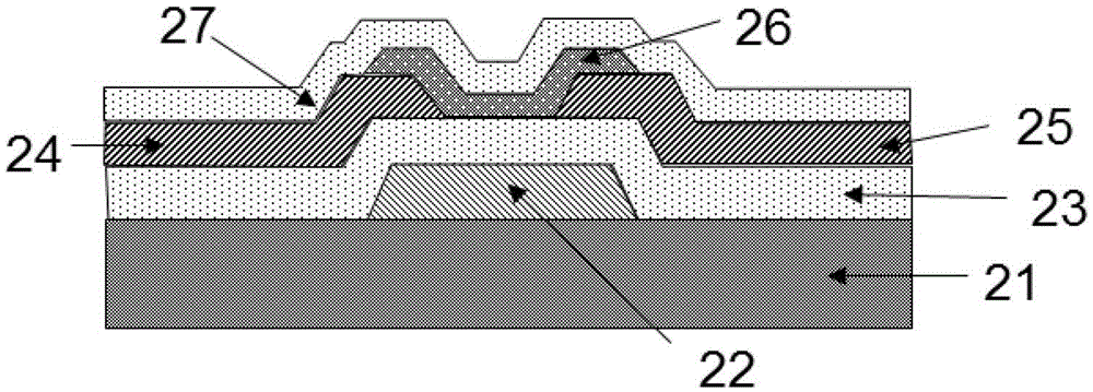
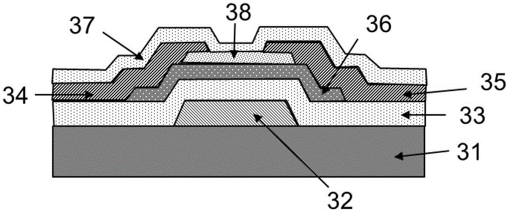
[0030] The invention discloses a semiconductor device, Figure 3 to Figure 3 (e) is a schematic diagram of the first embodiment of the present invention, such as image 3 As shown, the present semiconductor device includes from bottom to top: a gate 20 pattern on the base substrate 10, a gate insulating layer 30 covering the gate 20, a metal oxide semiconductor 40 on the gate insulating layer 30, Two conductive contact layers 70 and Al 2 o 3 The stacked pattern of the ...


PUM


Abstract

The invention provides a semiconductor device and a manufacture method thereof. The semiconductor device comprises a bottom substrate, a grid electrode, a grid electrode insulating layer, a metal oxide semiconductor layer, two conducting contact layers, a laminated structure of a metal oxide insulating layer, a source electrode, a drain electrode and a channel region. The conducting contact layers are located among the source electrode, the drain electrode and the metal oxide semiconductor layer, and the metal oxide insulating layer is located in the channel region. The conducting contact layers or manganese oxide layers of the semiconductor device are formed among the source electrode, the drain electrode and the metal oxide semiconductor layer through technological conditions including high temperature and the like and ensure the semiconductor device to lead a current carrier of the metal oxide semiconductor layer to the source electrode or the drain electrode in a working state. The manufacture method of the semiconductor device adopts a triple photolithographic process to manufacture an ESL functional structure. Compared with an existing quartic process, technological processes are simplified, a manufacture period of the device is shortened, and other negative factors brought by existing manufacture processes are avoided.

Description

technical field [0001] The invention relates to a semiconductor device with relatively high carrier mobility and a manufacturing method thereof, which is mainly used as a thin film transistor for driving a flat panel display, and can also be applied to other fields such as integrated circuits. Background technique [0002] Flat panel displays dominated by thin-film transistor liquid crystal displays (TFT-LCDs) continue to challenge indicators such as high-definition and high-frequency drive in order to meet the requirements of high-quality images. Considering the factor of increasing the size of the substrate, higher requirements are placed on the electron mobility of TFTs for next-generation flat panel displays. [0003] At present, the amorphous silicon (a-Si: AmorphousSilicon) TFT that supports the development of TFT-LCD can no longer meet the requirements of new technologies. Although the electron mobility of low-temperature polysilicon (LTPS: LowTemperaturePoly-Silicon)...

Claims


Application Information

Patent Timeline
Patent Type & Authority Patents(China)
IPC IPC(8): H01L29/786H01L21/336
Inventor 马群刚
Owner NANJING CEC PANDA LCD TECH
Why Eureka
Try Eureka