Circuit arrangement and method for reducing common-mode noise in a switched-mode power supply, and a switched-mode power supply
A switching mode power supply and circuit layout technology, applied in the direction of output power conversion devices, electrical components, etc., can solve problems such as inefficiency
- Summary
- Abstract
- Description
- Claims
- Application Information
AI Technical Summary
Problems solved by technology
Method used
Image
Examples
Embodiment Construction
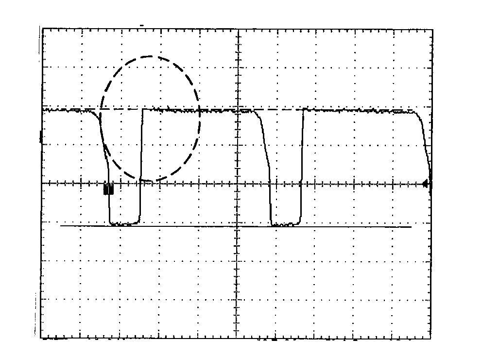
[0040] Examples of typical primary and secondary voltage waveforms are shown in Figures 1 and 2, respectively. The primary voltage waveform includes the overshoot that occurs when the primary stops conducting. The overshoot is depicted by the dotted circle in FIG. 1 . The secondary voltage waveform does not include such an overshoot as can be seen in FIG. 2 .
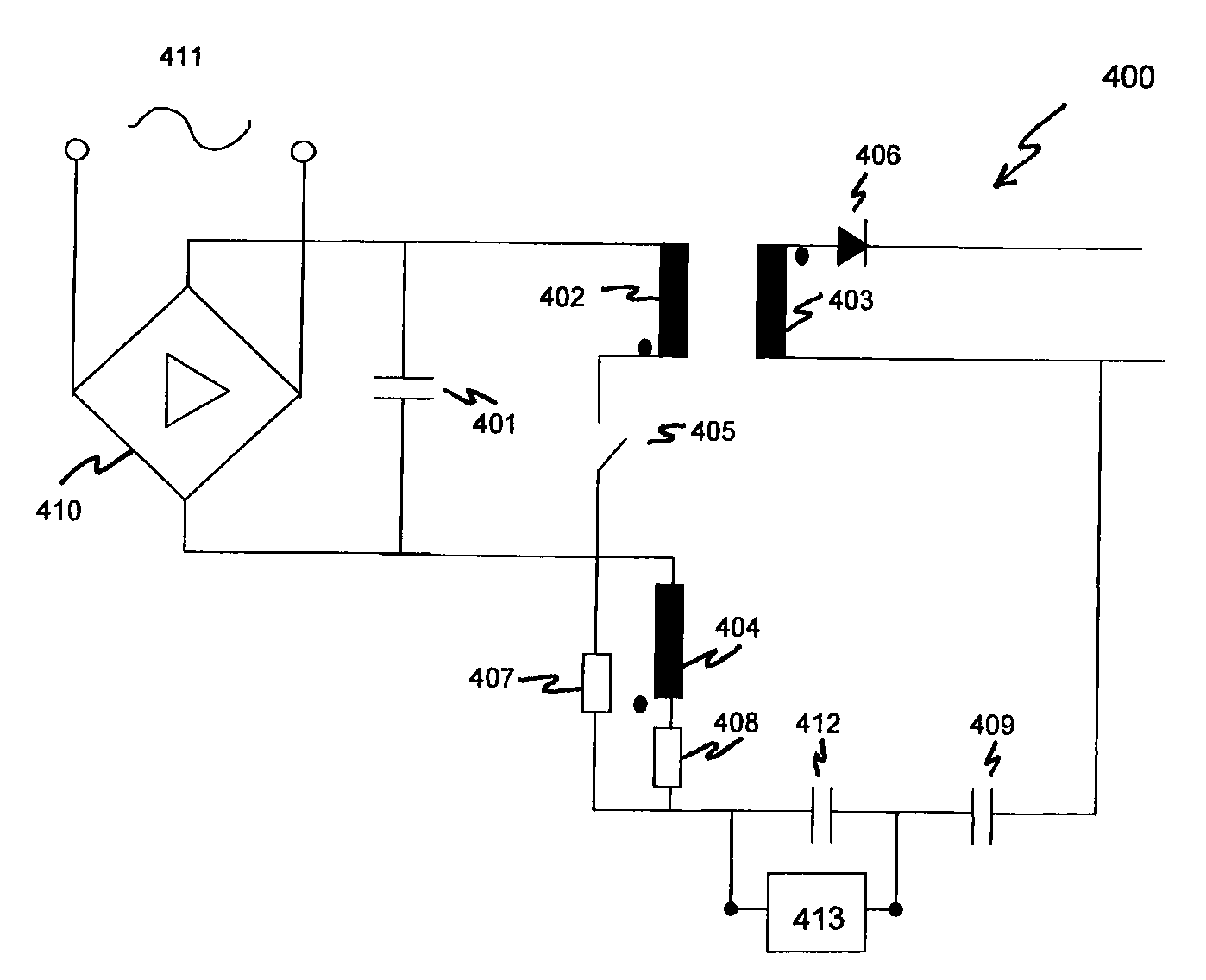
[0041] FIG. 3 is a schematic diagram of a flyback type switch mode power supply according to a first embodiment of the present invention. The flyback power supply 300 includes a primary filter capacitor 301 , a primary switch 305 , a transformer with a primary winding 302 , a secondary winding 303 and an auxiliary winding 304 , and a rectifier diode 306 . Windings 302, 303 and 304 are inductively coupled through a transformer. The auxiliary winding 304 is connected to a stable potential in the primary side, in this case to a primary filter capacitor 301 , which in turn is connected to the primary winding 302 . The p...
PUM
 Abstract
Description
Claims
Application Information
 - R&D
- Intellectual Property
- Life Sciences
- Materials
- Tech Scout
- Unparalleled Data Quality
- Higher Quality Content
- 60% Fewer Hallucinations
Browse by: Latest US Patents, China's latest patents, Technical Efficacy Thesaurus, Application Domain, Technology Topic, Popular Technical Reports.
© 2025 PatSnap. All rights reserved.Legal|Privacy policy|Modern Slavery Act Transparency Statement|Sitemap|About US| Contact US: help@patsnap.com


