
Manufacture method for gold finger circuit board and circuit board manufactured by method

A manufacturing method and gold finger technology, which is applied in the directions of printed circuit components, electrical connection printed components, and printed component electrical connection formation, etc., can solve the problems that the depth cannot be accurately controlled, and the unfavorable circuit board manufacturing accuracy requirements, etc., achieve simple process Effect

Active Publication Date: 2013-06-12
DONGGUAN SHENGYI ELECTRONICS
View PDF5 Cites 41 Cited by
  • Summary
  • Abstract
  • Description
  • Claims
  • Application Information

AI Technical Summary

Problems solved by technology

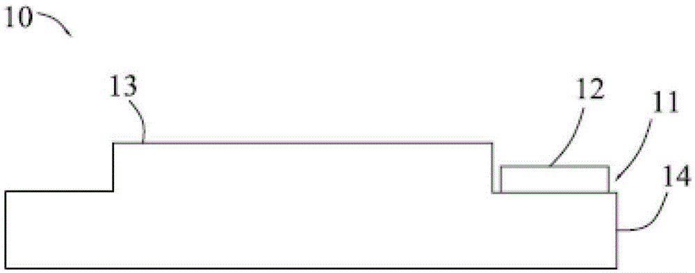
However, according to the demand of the market, there is a need to have a circuit board with stepped grooves and gold fingers arranged in the stepped grooves. How to prepare a circuit board that requires golden fingers to be arranged in the stepped grooves? The milling machine with milling function (optical scale control or conductive control) is directly machined and manufactured; by milling the stepped groove, and then performing surface treatment on the bottom of the stepped groove to make gold fingers; however, the depth of this method of controlling the depth of the milling plate cannot be precisely controlled , which is not conducive to the production accuracy requirements of the circuit board

Method used


Image

  • Manufacture method for gold finger circuit board and circuit board manufactured by method
  • Manufacture method for gold finger circuit board and circuit board manufactured by method
  • Manufacture method for gold finger circuit board and circuit board manufactured by method

Examples


Embodiment Construction

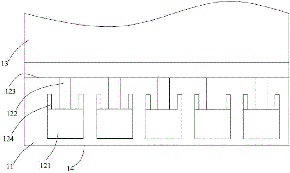
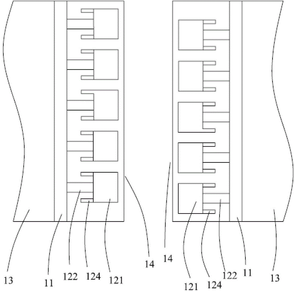
[0030] In order to elaborate the technical solutions adopted by the present invention to achieve the predetermined technical purpose, the technical solutions in the embodiments of the present invention will be clearly and completely described below with reference to the accompanying drawings in the embodiments of the present invention. Obviously, the described implementation The examples are only some of the embodiments of the present invention, not all of the embodiments, and the technical means or technical features in the embodiments of the present invention can be replaced without creative work. The following will refer to the accompanying drawings in conjunction with Examples are given to illustrate the present invention in detail.

[0031] see Figure 1 to Figure 7 , the manufacturing method of the golden finger circuit board of the present invention, the manufacturing method comprises the following steps:

[0032] Step 1 , providing a substrate 10 with a stepped groove...


PUM


Abstract

The invention provides a manufacture method for a gold finger circuit board and the circuit board manufactured by the method. The manufacture method for the gold finger circuit board comprises the steps of offering a base board with a ladder groove, manufacturing a gold finger structure inside the ladder groove, wherein the gold finger structure comprises a gold finger figure and a lead wire connected with the gold finger figure, covering heat resisting solder resisting ink on the surface of the lead wire, coating heat resisting adhesive tape on the surface of the gold finger figure in an attached mode, offering a plurality of plates which are arranged inside the ladder groove in a stack mode, pressing the plurality of plates in a fit mode, milling a top plate corresponding to the adhesive tape in the stacked plates, taking out a sandwich plate clamped between the plate at the top of the plates and the heat resisting adhesive tape, removing the heat resisting adhesive tape covered on the surface of the gold finger figure, electroplating the gold finger figure, forming a gold finger, and obtaining the required gold finger circuit board. The manufacture method can accurately manufacturing the thickness of the required circuit board, can achieve manufacture of the gold finger inside the ladder groove, and is simple in process.

Description

technical field [0001] The invention relates to a circuit board manufacturing method, in particular to a circuit board manufacturing method with stepped grooves and gold fingers arranged in the stepped grooves and a circuit board obtained by the method. Background technique [0002] Gold fingers are composed of golden yellow conductive sheets arranged on the circuit board and arranged in an array, which are used to be plugged into the slot of another component and electrically conductive with another component. Gold fingers are called gold fingers because their surfaces are gold-plated and the conductive sheets are arranged like fingers. The gold finger is actually a layer of gold on the copper clad plate by electroplating or chemical plating. Because the gold finger made by chemical plating is hard, the gold finger is easily broken by external force; the gold finger made by electroplating Fingers do not have the above-mentioned defects, so the industry adopts electroplatin...

Claims


Application Information

Patent Timeline
Patent Type & Authority Applications(China)
IPC IPC(8): H05K3/40H05K1/11
Inventor 王小平焦其正杜红兵李恢海吕红刚
Owner DONGGUAN SHENGYI ELECTRONICS
Learn More