Method for forming a shape of an electro-optical component or photovoltaic component
A technology of optoelectronic components and electro-optical components, which is applied in metal processing and other directions, and can solve the problem that diamond grinding discs cannot have precise details of the outer contour and edges.
- Summary
- Abstract
- Description
- Claims
- Application Information
AI Technical Summary
Problems solved by technology
Method used
Image
Examples
Embodiment Construction
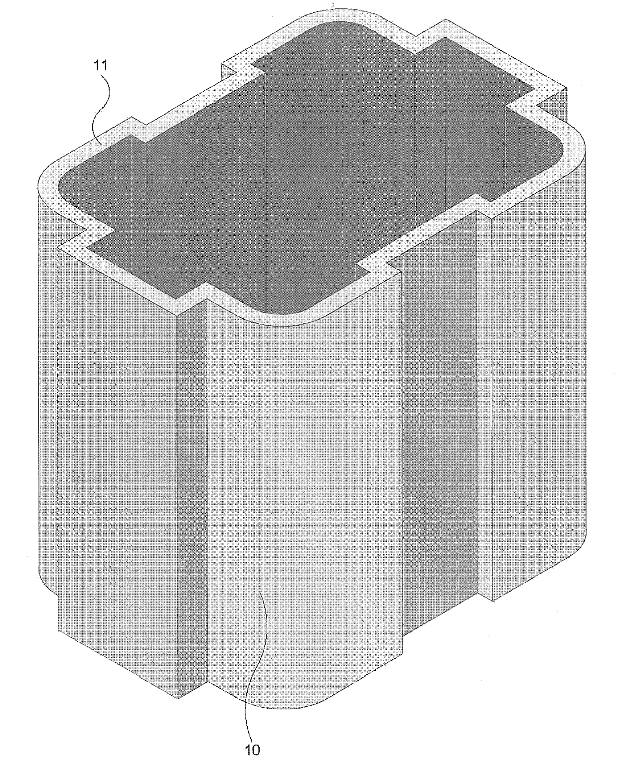
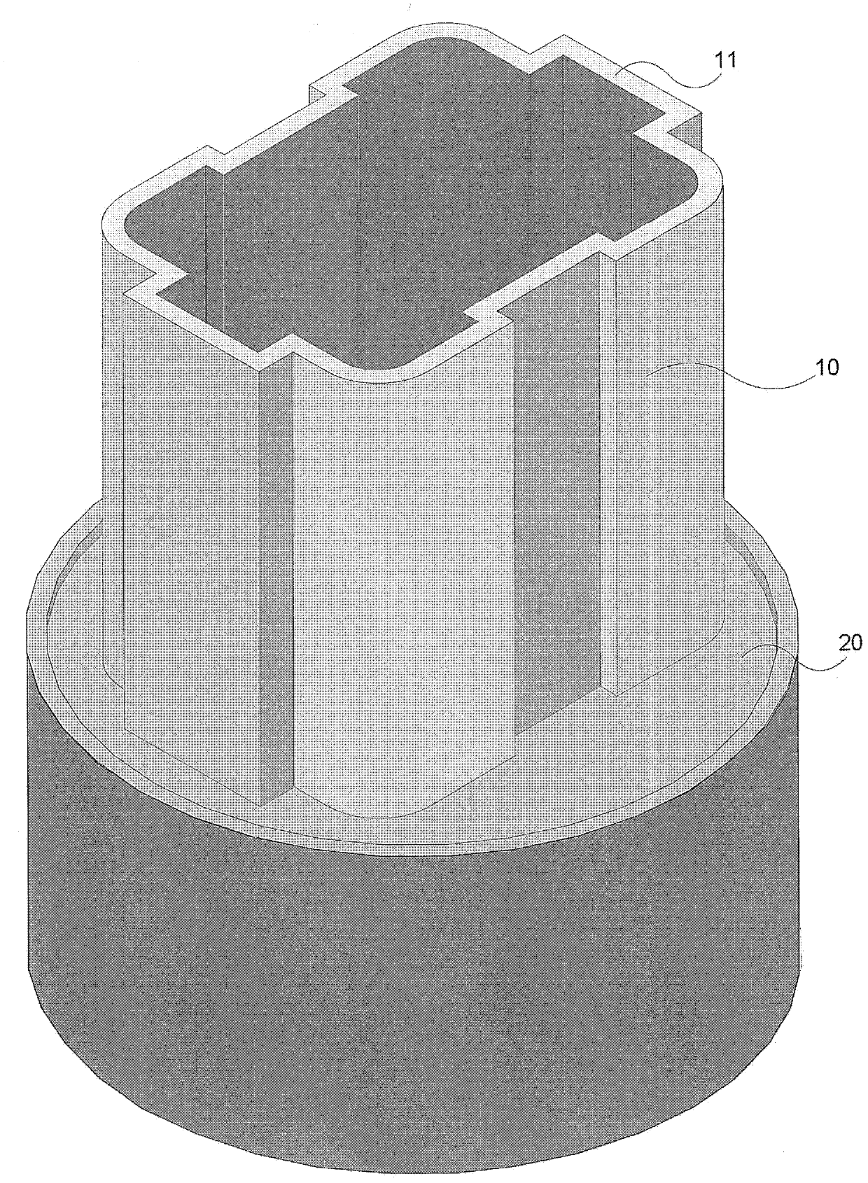
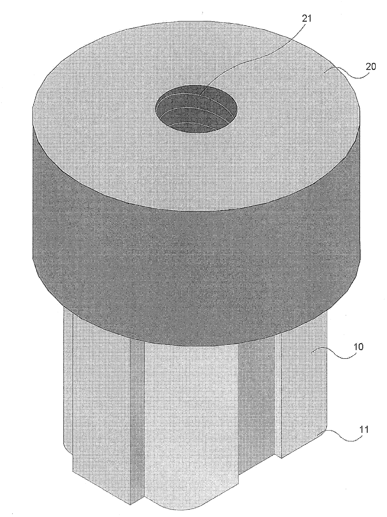
[0030] Referring to the drawings, a method for forming the shape of the electro-optical element 59 or the photovoltaic element 59 is provided. The method generally includes ultrasonically cutting the substrate 40 using an ultrasonic cutter. The ultrasonic cutting machine has a stand adapter 20 . The stand adapter 20 is operatively connected to the forming die 10 . The forming die 10 has a contact edge 11 corresponding to the final shape of the electro-optical or optoelectronic component. The contact edge 11 is generally a flat surface. The contact edge 11 is in contact with the substrate 40 at a contact region 42 . The method also includes spraying abrasive fluid 42 onto contact area 42 while the ultrasonic cutter is operating. After the substrate 40 is ultrasonically cut for a predetermined amount of time, the element 59 having a shape corresponding to the contact edge 11 of the forming die 10 is formed.
[0031] The method enables the formation of irregular shapes of el...
PUM
| Property | Measurement | Unit |
|---|---|---|
| height | aaaaa | aaaaa |
Abstract
Description
Claims
Application Information
 - R&D
- Intellectual Property
- Life Sciences
- Materials
- Tech Scout
- Unparalleled Data Quality
- Higher Quality Content
- 60% Fewer Hallucinations
Browse by: Latest US Patents, China's latest patents, Technical Efficacy Thesaurus, Application Domain, Technology Topic, Popular Technical Reports.
© 2025 PatSnap. All rights reserved.Legal|Privacy policy|Modern Slavery Act Transparency Statement|Sitemap|About US| Contact US: help@patsnap.com


