Method and system for determining surface appearances of aluminum metal gate chips

An aluminum metal and chip technology, applied in the field of semiconductor manufacturability design, can solve the problems of difficult aluminum gate planarization process, extremely demanding CMP process requirements, and inability to accurately reflect the grinding effect of the CMP process, so as to reduce costs and shorten process adjustment. effect of cycles

Active Publication Date: 2013-05-29
INST OF MICROELECTRONICS CHINESE ACAD OF SCI
View PDF5 Cites 6 Cited by
  • Summary
  • Abstract
  • Description
  • Claims
  • Application Information

AI Technical Summary

Problems solved by technology

[0004]At present, the core technology of the CMP process result determination method of the mainstream manufacturers in the relatively mature semiconductor industry is mainly for the CMP process of copper, and when aluminum is used as the gate material The deposition thickness is relatively thin, and the requirements for the CMP process are extremely strict. The existing methods for determining the results of the CMP process for copper are difficult to directly apply to the planarization process of the aluminum gate.
The CMP process control of major domestic chip manufacturers for aluminum gates mainly relies on empirical methods. Generally, the experimental results are used to predict the grinding results of chips under the same grinding conditions. The impact of the flatness and wafer removal rate, the prediction results cannot accurately reflect the grinding effect of the CMP process
Especially in the nano-scale node chip manufacturing process, the flatness of the surface is extremely high, and the chemical effect of abrasive particles plays a more prominent role in grinding and removal. The interaction between the polishing pad, the polishing liquid and the chip surface is an extremely complicated process. Empirical methods cannot simply be used to describe the topography of aluminum metal gate surfaces after CMP grinding

Method used


Image

  • Method and system for determining surface appearances of aluminum metal gate chips
  • Method and system for determining surface appearances of aluminum metal gate chips
  • Method and system for determining surface appearances of aluminum metal gate chips

Examples


Embodiment Construction

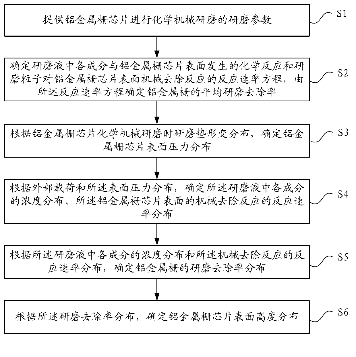
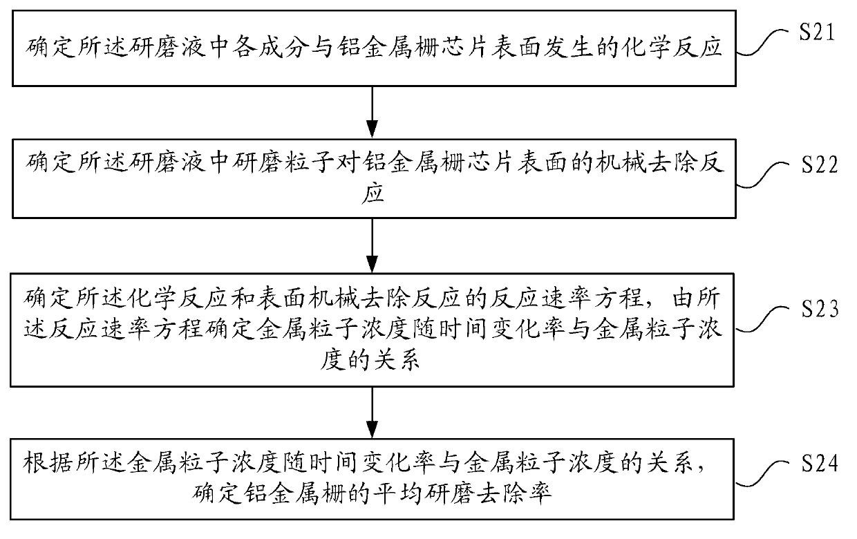
[0050] The following will clearly and completely describe the technical solutions in the embodiments of the present invention with reference to the drawings in the embodiments of the present invention. Apparently, the described embodiments are only some of the embodiments of the present invention, but not all of them. Based on the embodiments of the present invention, all other embodiments obtained by persons of ordinary skill in the art without making creative efforts belong to the protection scope of the present invention.

[0051] Secondly, the present invention is described in detail with reference to the schematic diagrams. When describing the embodiments of the present invention in detail, for the convenience of explanation, the schematic diagrams are only examples, which should not limit the protection scope of the present invention.

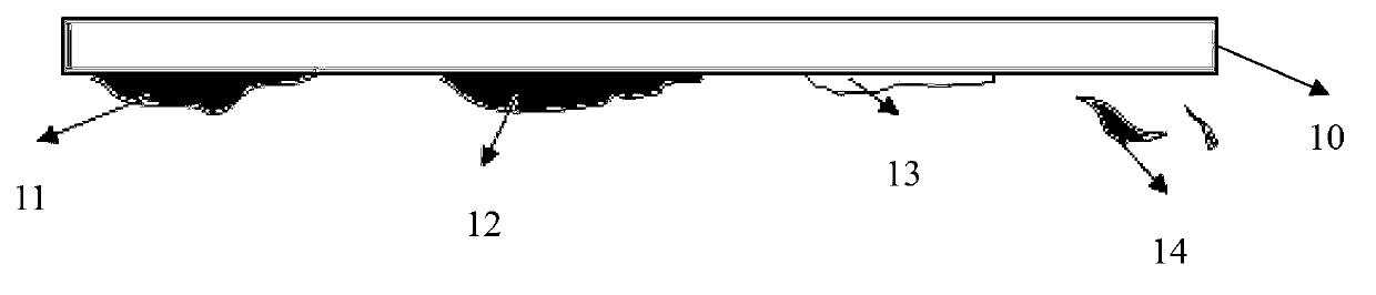
[0052] As mentioned in the background technology, the core technology of the mainstream CMP process result determination method in the s...


PUM


Abstract

The invention provides a method and a system for determining surface appearances of aluminum metal gate chips. The method comprises determining an average polishing removal rate of aluminum metal gates according to polishing parameters of chemical machinery, chemical reactions between components in a polishing liquid and the surface of an aluminum metal gate chip and a reaction rate equation of the mechanical removal reaction of polishing particles to the chip surface; determining pressure distribution of the aluminum metal gate chip surface according to polishing pad deformation distribution of the aluminum metal gate chip during chemical mechanical polishing, and then determining concentration distribution of the components in the polishing liquid, reaction rate distribution of the mechanical removal reaction of the surface of the aluminum metal gate chip, and determining polishing removal rate distribution of the aluminum metal gates finally; and determining height distribution of the surface of the aluminum metal gate chip according to the polishing removal rate distribution. According to the method and the system for determining surface appearances of the aluminum metal gate chips, effective polishing particle mechanical removal, chemical kinetic removal of the polishing liquid towards the chips and pressure distribution of the aluminum metal gate chip surface in the polishing process are considered comprehensively, and accordingly, aluminum metal gate surface appearances can be determined accurately.

Description

technical field [0001] The invention relates to the technical field of semiconductor manufacturability design, in particular to a method and a system for determining the surface topography of an aluminum metal gate chip during chemical mechanical polishing. Background technique [0002] High-k gate dielectric and metal gate technology (HKMG, High-k Metal Gate) as the mainstream process technology at the 32 or 28 nanometer node makes the development of the semiconductor industry still follow the Moore that the integration of chips doubles every 18 months law. As the chip node size continues to decrease, in the chip manufacturing process, the flatness of the chip surface is an important factor affecting the subsequent manufacturing process and chip yield. Chemical Mechanical Polishing (CMP, Chemical Mechanical Polishing) process, as a reliable method to achieve chip surface planarization in manufacturability design, has been widely used in the ultra-fine surface planarization...

Claims


Application Information

Patent Timeline
Patent Type & Authority Applications(China)
IPC IPC(8): H01L27/02
Inventor 徐勤志陈岚
Owner INST OF MICROELECTRONICS CHINESE ACAD OF SCI
Why Eureka
Try Eureka