A method for electroplating and filling holes on pads

A technology of electroplating filling holes and conducting holes, which is applied in the direction of electrical connection formation of printed components, can solve the problems of reducing the high precision and high density of mechanical blind plate holes, complex processes, etc., and achieve the effect of improving product quality and enhancing high precision

Active Publication Date: 2016-05-04
金悦通电子(翁源)有限公司
View PDF10 Cites 0 Cited by
  • Summary
  • Abstract
  • Description
  • Claims
  • Application Information

AI Technical Summary

Problems solved by technology

[0005] The Chinese invention patent discloses a patent application number: 201110101403.1, the invention name is: high thickness-to-diameter ratio backplane resin plugging method, and a process flow is disclosed: pre-process→pressing→drilling holes that require resin plug holes And aluminum sheet, air-permeable plate processing → sinking copper, plate plating → optical imaging → plating hole → resin plug hole → pre-curing → grinding → QC inspection → curing → drilling other holes → post-process, the invention patent has some parameters and processes The process is optimized, and a resin plugging process that can achieve a thickness-to-diameter ratio of 15:1 is revealed. This process first deposits copper, plated the plate, and then performs resin plugging, pre-curing and curing, which reduces mechanical blindness. High precision and high density of plate holes, and the process is complex

Method used


Image

  • A method for electroplating and filling holes on pads
  • A method for electroplating and filling holes on pads

Examples


Embodiment Construction

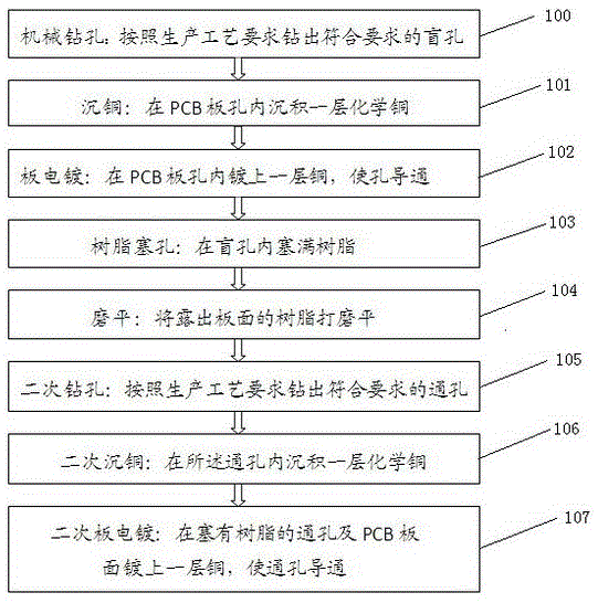
[0022] In the embodiment of the present invention, the preliminary shape of the hole is formed by mechanical drilling, resin plugging, grinding, and secondary copper sinking, and then the secondary plate is used to fill the hole, which enhances the high precision, high density, and high precision of the mechanical blind hole plate. Reliability and other performances have achieved the production requirements of PCB boards with high thickness-to-diameter ratios and improved product quality.

[0023] see figure 1 , which is a schematic flowchart of a method for electroplating and filling via holes on pads provided by the present invention.

[0024] This embodiment provides a method for electroplating and filling via holes on pads, including:

[0025] Step 100, mechanical drilling: drilling blind holes that meet the requirements according to the production process requirements;

[0026] Step 101, sinking copper: depositing a layer of chemical copper in the hole of the PCB;

[0...


PUM


Abstract

The invention provides an electroplating hole filling method for a via hole on a bonding pad. The electroplating hole filling method for the via hole on the bonding pad comprises the following sequentially executed steps: machine drilling: drilling a blind hole which meets the requirement according to production process requirements, depositing copper: depositing a layer of chemical copper in a hole of a printed circuit board (PCB), board electroplating: electroplating a layer of copper in the hole of the PCB, and breaking through the hole, plugging hole with resin: plugging the blind hole with resin, polishing flat: polishing the resin exposed from the board to be flat, secondary drilling, drilling a through hole which meets the requirement according to the production process requirements, secondary depositing copper: depositing a layer of chemical copper in the through hole, and secondary board electroplating: electroplating a layer of copper in the through hole which is plugged with resin and the surface of the PCB, and breaking through the hole. High precision, high density and high reliability of hole filling board technology of the via hole on the bonding pad are enhanced and the blank of mechanical blind hole boards is filled, product quality is increased and production of the PCB with high thickness-diameter ratio is achieved.

Description

technical field [0001] The invention relates to the technical field of PCB boards, in particular to a method for electroplating and filling via holes on pads. Background technique [0002] PCB (Printed Circuit Board), the Chinese name is printed circuit board, referred to as printed board, is one of the important components of the electronics industry. Almost every kind of electronic equipment, ranging from electronic watches and calculators to computers, communication electronic equipment, and military weapon systems, as long as there are electronic components such as integrated circuits, printed boards are used for the electrical interconnection between them. . [0003] With the high demand and development of PCB boards, high-density internal connection printed circuit boards (HDI) are increasingly showing their superiority, and are widely used in mobile phones, GPS, DV, notebook computers and other portable consumer electronics product. However, with the continuous upg...

Claims


Application Information

Patent Timeline
Patent Type & Authority Patents(China)
IPC IPC(8): H05K3/42
Inventor 胡俊
Owner 金悦通电子(翁源)有限公司
Why Eureka
Try Eureka