Graphene transistor based on metamaterial structure, optical sensor based on metamaterial structure, and application of graphene transistor

A technology of metamaterials and transistors, applied in the field of photodetection devices

Active Publication Date: 2013-05-22
SUZHOU INST OF NANO TECH & NANO BIONICS CHINESE ACEDEMY OF SCI
View PDF3 Cites 75 Cited by
  • Summary
  • Abstract
  • Description
  • Claims
  • Application Information

AI Technical Summary

Problems solved by technology

It can be seen that graphene-based detectors have demonstrated an ultra-wide working range from visible light to terahertz waves, although the above-mentioned technologies have demonstrated a certain degree of graphene light absorption performance improvement through microcavity or plasmon effects. , however, the complexity of the technical process and the limitations of performance improvement require the industry to further explore more effective technical solutions

Method used


Image

  • Graphene transistor based on metamaterial structure, optical sensor based on metamaterial structure, and application of graphene transistor
  • Graphene transistor based on metamaterial structure, optical sensor based on metamaterial structure, and application of graphene transistor
  • Graphene transistor based on metamaterial structure, optical sensor based on metamaterial structure, and application of graphene transistor

Examples


Embodiment 1

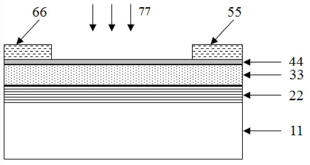
[0051] Example 1: refer to figure 1 Shown is the longitudinal cross-sectional view of the graphene transistor photodetector based on the metamaterial structure of this embodiment, which includes a substrate 11, a gate metal layer 22, a gate dielectric layer 33, a graphene layer 44, a source 55 and a drain 66 metal layers, the incident light is shown by the arrow 77 in the figure. In this embodiment, the gate metal layer 22 constitutes the reflective layer of the metamaterial, and the metal layers of the source electrode 55 and the drain electrode 66 constitute the surface impedance matching layer of the metamaterial. By optimizing the design of the gate dielectric layer 33 and the source electrode 55 and the drain electrode 66 The periodic structure can get nearly complete absorption of the preset band. At the same time, the gate metal layer 22 can be used as the gate of the transistor to regulate the forbidden band of the graphene layer 44 and form a carrier conduction ch...

Embodiment 2

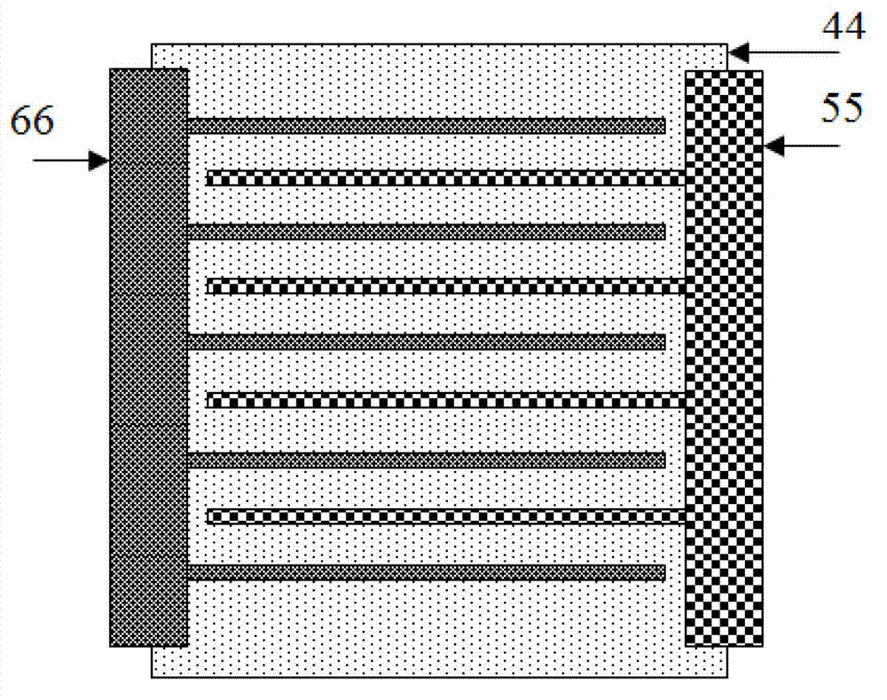
[0052] Example 2: The longitudinal sectional view of this embodiment can refer to figure 1 , top view diagram see image 3 , the main difference from Embodiment 1 is that in this embodiment, the source 55 and the drain 66 form a two-dimensional periodic structure, and the surface impedance matching layer of the metamaterial formed by it can form a Near-zero reflection, thereby further improving the photoelectric conversion efficiency of the detector.

Embodiment 3

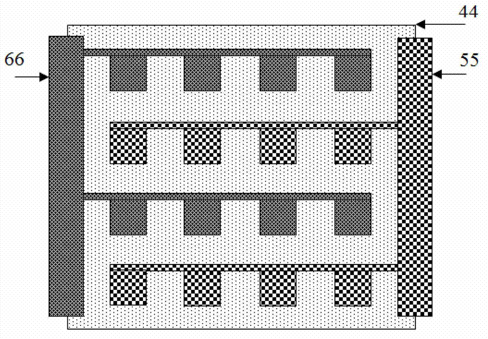
[0053] Example 3: refer to Figure 4 Shown is the schematic diagram of the top view of the graphene transistor photodetector based on the metamaterial structure in this embodiment for imaging applications, wherein A, B, C, and D are respectively graphene transistor photodetectors working in different preset wavebands. It can be either of Embodiment 1 and Embodiment 2. By integrating A, B, C, and D detectors into one pixel I and periodically arranging them to form the entire image sensor, multi-band imaging can be obtained. For example, A and D are graphene transistor photodetectors in blue and red bands respectively, and B and C are graphene transistor photodetectors in green band, which constitute an RGB (red, green and blue) color image sensor. By optimizing various integration schemes of graphene transistor photodetectors in different bands, a multi-band combined super camera can be obtained.


PUM

PropertyMeasurementUnit
impedanceaaaaaaaaaa

Abstract

Disclosed are a graphene transistor based on a metamaterial structure, an optical sensor based on a metamaterial structure, and application of the graphene transistor. The graphene transistor sequentially comprises a liner, a grid metal layer, a grid medium layer, a grapheme layer and a source and drain metal layer from bottom to top. At least local area of the source and drain metal layer is provided with a periodicity micro-nano structure. The periodicity micro-nano structure, the grid metal layer and the grid medium layer match to form the metamaterial structure with the feature of complete absorption. By changing refractive index, thickness and the like of the periodicity micro-nano structure and the grid medium layer material, optical absorption frequency range of the metamaterial structure can be adjusted. Due to the feature of perfect wavelength selectivity absorption, higher flexibility and narrow-band response of the metamaterial structure, the graphene transistor can work under visible light to infrared even longer wave bands by selecting different metamaterial structures. By integrating optical sensor working in different wave bands, image sensors, spectrum detecting analyzing device and the like which can work in ultra-wide bands can be formed.

Description

technical field [0001] The invention relates to a photodetection device, in particular to a graphene field-effect transistor based on micro-nano structure-enhanced absorption, a photodetector and its imaging application. Background technique [0002] Graphene is a two-dimensional layered material structure of carbon elements. The thickness of a single layer of graphite is about 0.35 nanometers, and it has extraordinary electrical, optical and mechanical properties. Graphite with less than ten layers is considered graphene. Since single-layer graphene was successfully developed in 2004, graphene has attracted widespread attention. Due to its Dirac-Fermi properties, graphene has a linear energy band structure and has the highest carrier mobility (200000cm 2 V -1 the s -1 ), so it is widely used in the field of high-frequency nanoelectronic devices. Graphene also has extraordinary optical properties, with flat absorption bands in the ultraviolet, visible and infrared bands...

Claims


Application Information

Patent Timeline
Patent Type & Authority Applications(China)
IPC IPC(8): H01L31/028H01L31/0224G01J3/02G01J3/28
CPCH01L31/0224H01L31/028H01L27/146H01L31/02162H01L31/1136H01L29/0847H01L29/1606H01L29/42372Y02E10/547
Inventor 陈沁
Owner SUZHOU INST OF NANO TECH & NANO BIONICS CHINESE ACEDEMY OF SCI
Why Eureka
Try Eureka