


Quick Research
Generate reliable direction feasibility study reports for your R&D in just a few steps.

Technical Q&A
Discover and master advanced knowledge NOW. Basics, ideas, possibilities, all at once.

Find Solutions
As an expert in R&D theories, this can generate solutions to your technical problems instantly.

Evaluate Feasibility
Analyze your overall solution with one click, know your potential R&D risks in advance.

Monitor Landscape
Get weekly tech updates, stay abreast of the latest tech innovations and key insights.
Manufacturing method of array substrate, array substrate and display device
A technology of an array substrate and a manufacturing method, applied in the fields of array substrates and display devices, can solve the problems affecting production efficiency, high exposure energy, and reduce exposure speed, and achieve the effects of improving production efficiency, increasing exposure speed, and reducing exposure energy.
- Summary
- Abstract
- Description
- Claims
- Application Information
AI Technical Summary
Problems solved by technology
Method used
Image


Examples
Embodiment Construction
[0039] In order to make the technical problems, technical solutions and advantages to be solved by the present invention clearer, the following will describe in detail with reference to the drawings and specific embodiments.
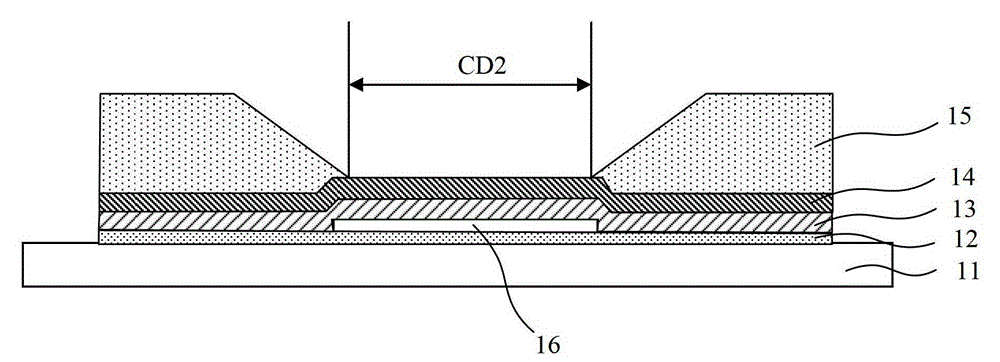
[0040] An embodiment of the present invention provides a method for manufacturing an array substrate, including: forming a pad layer on the array substrate, the pad layer is located under the planarization layer of the array substrate and corresponds to the position of the via hole in the planarization layer , wherein, the planarization layer is formed of hot-melt material. The hot-melt material is a material that has fluidity when heated to a certain temperature.
[0041] Specifically, the manufacturing method of the array substrate includes:
[0042] A base substrate is provided, a TFT is formed on the base substrate; a planarization layer is formed above the TFT, and a via hole is formed on the planarization layer; a pad layer is formed on the array ...
PUM
 Abstract
Description
Claims
Application Information
 - R&D Engineer
- R&D Manager
- IP Professional
- Industry Leading Data Capabilities
- Powerful AI technology
- Patent DNA Extraction
Browse by: Latest US Patents, China's latest patents, Technical Efficacy Thesaurus, Application Domain, Technology Topic, Popular Technical Reports.
© 2024 PatSnap. All rights reserved.Legal|Privacy policy|Modern Slavery Act Transparency Statement|Sitemap|About US| Contact US: help@patsnap.com