A bonding machine device and a bonding alignment method

A bonding machine and bonding technology, used in electrical components, semiconductor/solid-state device manufacturing, circuits, etc., can solve problems such as low alignment, long alignment time, and low image sensor yield, and achieve improved Yield, time reduction, and the effect of precise alignment process

Active Publication Date: 2015-09-09
WUHAN XINXIN SEMICON MFG CO LTD
View PDF10 Cites 2 Cited by
  • Summary
  • Abstract
  • Description
  • Claims
  • Application Information

AI Technical Summary

Problems solved by technology

[0004] The technical problem to be solved by the present invention is to provide a bonding machine device and a bonding alignment method to solve the problem of low alignment in the bonding process in the prior art, which leads to low yield rate of image sensors and long alignment time. question

Method used


Image

  • A bonding machine device and a bonding alignment method
  • A bonding machine device and a bonding alignment method

Examples


Embodiment Construction

[0030] The principles and features of the present invention are described below in conjunction with the accompanying drawings, and the examples given are only used to explain the present invention, and are not intended to limit the scope of the present invention.

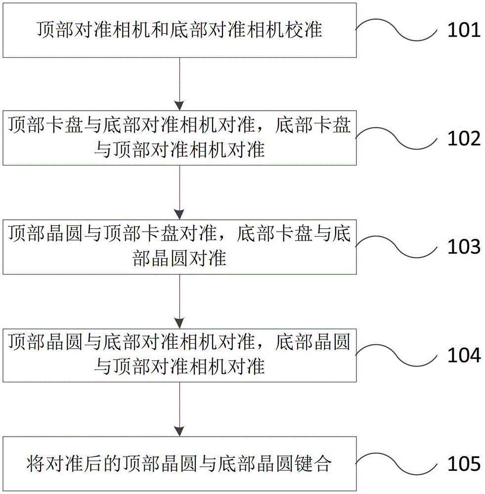
[0031] Such as figure 1 Shown, be the method flowchart of the present invention, its concrete steps are as follows:

[0032] Step 101, aligning the top alignment camera on the bonding machine table with the standard alignment mark on the bonding machine table, and aligning the bottom alignment camera with the standard alignment mark on the bonding machine table;

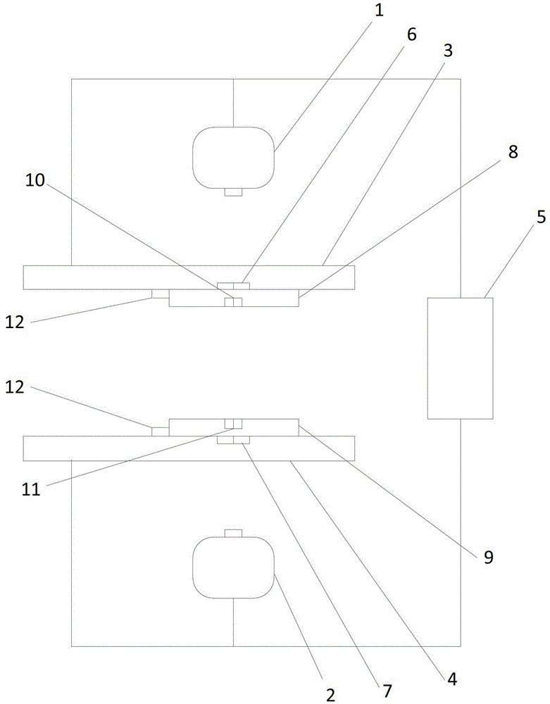
[0033] Step 102, move the top chuck on the bonding machine table to align the top chuck alignment mark provided on the top chuck with the bottom alignment camera, and move the bottom chuck on the bonding machine table to align the top chuck alignment mark provided on the top chuck with the bottom alignment camera. The bottom chuck alignment mark provided ...


PUM


Abstract

The invention relates to a bonding technology for semiconductor manufacture, in particular to a bonding machine device and a bonding alignment method. The bonding alignment method comprises the following steps of: aligning a top alignment camera and a bottom alignment camera with a standard alignment identifier respectively; aligning a top chuck alignment identifier with the bottom alignment camera, and aligning a bottom chuck alignment identifier with the top alignment camera; aligning a top wafer alignment identifier with the top chuck alignment identifier; aligning a bottom wafer alignment identifier with the bottom chuck alignment identifier; aligning the top wafer alignment identifier with the bottom alignment camera, and aligning the bottom wafer alignment identifier with the top alignment camera; and bonding a top wafer and a bottom wafer, which are aligned. According to the bonding machine device and the bonding alignment method, an unknown parameter that whether chucks are aligned or not is substantially eliminated, so that the wafers can be aligned more accurately to solve the problems of low image sensor yield and long alignment time caused by low alignment degree in a bonding process, further improve the yield of an image sensor, reduce the time of the whole bonding process and improve the production efficiency.

Description

technical field [0001] The invention relates to semiconductor manufacturing bonding technology, in particular to a bonding machine device and a bonding alignment method. Background technique [0002] In the manufacturing process of the back-illuminated image sensor, steps such as adding a metal shielding layer and an optical filter need to be performed after the device wafer and the logic wafer are bonded and the backside of the device wafer is thinned. The backside thinning process will bring about the removal of the alignment mark on the device wafer, which will affect the accuracy of lithography. The maximum allowable error of plus or minus 50 microns in mechanical alignment may cause errors in the lithography machine. To a large extent, it causes the loss of the yield rate of the image sensor and the problem of increasing the process time. [0003] The alignment method in the prior art is to first align the top alignment camera and the top alignment camera with the stan...

Claims


Application Information

Patent Timeline
Patent Type & Authority Patents(China)
IPC IPC(8): H01L21/60H01L21/68
Inventor 李平
Owner WUHAN XINXIN SEMICON MFG CO LTD
Why Eureka
Try Eureka