Power semiconductor device with antistatic discharge capacity and manufacturing method
A power semiconductor and discharge capability technology, applied in semiconductor/solid-state device manufacturing, semiconductor devices, electric solid-state devices, etc., can solve the problems of complex formation and increase cost, and achieve design flexibility, cost reduction, and improvement of ESD capability. Effect
- Summary
- Abstract
- Description
- Claims
- Application Information
AI Technical Summary
Problems solved by technology
Method used
Image
Examples
Embodiment 1
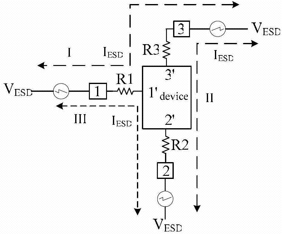
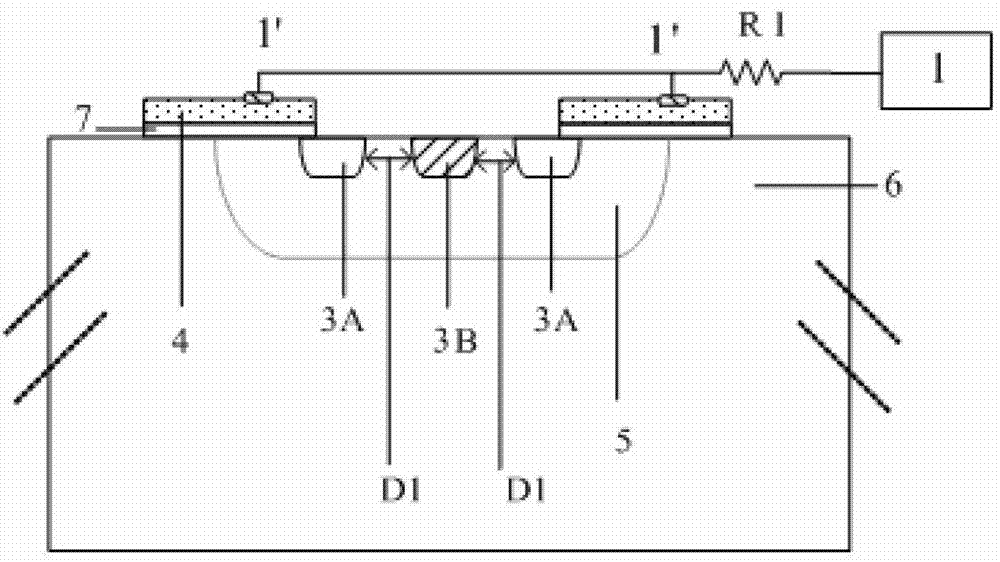
[0053] Figure 3 to Figure 5It shows that the present invention provides a power semiconductor device with anti-static discharge capability, and the gate terminal is connected in series with strip resistors to form a circular array layout structure of the gate.
[0054] Such as Figure 3 to Figure 5 As shown, the steps for forming each of the cells 8 are as follows: provide an epitaxial layer (not shown in the figure, please refer to Figure 2A to Figure 2C In the mark 6); form a second-type lightly doped region in the epitaxial layer (not shown in the figure, please refer to Figure 2A to Figure 2C Mark 5 in the above); on the epitaxial layer, a gate dielectric layer is sequentially formed from bottom to top (not shown in the figure, please refer to Figure 2A to Figure 2C Mark 7) and the first polysilicon strip 4; etch the first polysilicon strip 4 and the gate dielectric layer to expose the second-type lightly doped region; in the second-type lightly doped A first type h...
Embodiment 2
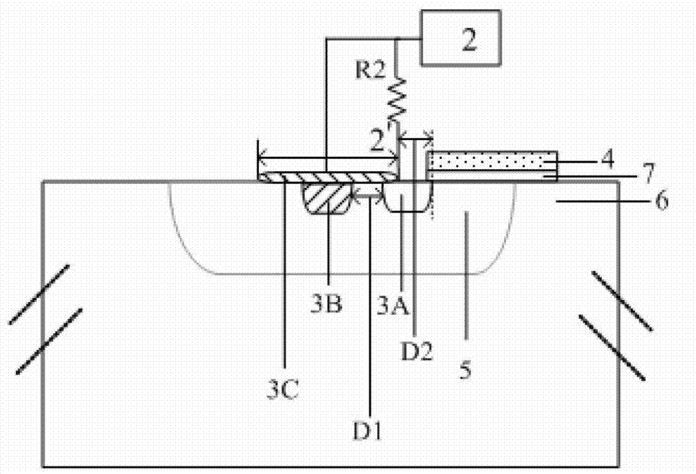
[0061] Figure 8 to Figure 9 Shown is the circular array layout structure of the source terminal of the power semiconductor device with anti-static discharge capability of the present invention, which is connected in series with strip resistors to form the source.
[0062] Such as Figure 8 and 9 As shown, the steps for forming each of the cells 8 are as follows: provide an epitaxial layer (not shown in the figure, please refer to Figure 2A to Figure 2C In the mark 6); form a second-type lightly doped region in the epitaxial layer (not shown in the figure, please refer to Figure 2A to Figure 2C Mark 5 in the above); on the epitaxial layer, a gate dielectric layer is sequentially formed from bottom to top (not shown in the figure, please refer to Figure 2A to Figure 2C Mark 7) and the first polysilicon strip 4; etch the first polysilicon strip 4 and the gate dielectric layer to expose the second-type lightly doped region; in the second-type lightly doped A first type hea...
Embodiment 3
[0072] Figure 12 The difference between the illustrated embodiment and the first and second embodiments is to provide a circular array layout structure in which the gate terminal and the source terminal of the power semiconductor device with anti-static discharge capability are simultaneously connected in series with resistors to form the gate and source.
[0073] In this embodiment, the changed embodiment 1 can be combined with the layout structure of embodiment 2 to form Figure 12 . The content of the changes in the first embodiment is as follows: a first port 1' is provided on the second polysilicon strip 4', and a second port 1' is provided on the second polysilicon strip 4' other than the first port 1' The gate 1 is formed, and the second polysilicon strip 4 ′ is a resistor R1 connected to the first port, and the first port 1 ′ has no direct electrical connection with the gate 1 . Then, the size of the resistor R1 connected in series with the gate terminal can be adju...
PUM
 Abstract
Description
Claims
Application Information
 - R&D
- Intellectual Property
- Life Sciences
- Materials
- Tech Scout
- Unparalleled Data Quality
- Higher Quality Content
- 60% Fewer Hallucinations
Browse by: Latest US Patents, China's latest patents, Technical Efficacy Thesaurus, Application Domain, Technology Topic, Popular Technical Reports.
© 2025 PatSnap. All rights reserved.Legal|Privacy policy|Modern Slavery Act Transparency Statement|Sitemap|About US| Contact US: help@patsnap.com


