Chip packaging structure of a plurality of assemblies

A chip packaging structure and multi-component technology, applied in the direction of electrical components, semiconductor devices, electric solid devices, etc., can solve the problems of large package thickness and adverse effects on chip performance, achieve thickness reduction, good electrical stability, and avoid negative effects effect of influence

Active Publication Date: 2013-03-27
HEFEI SMAT TECH CO LTD
View PDF9 Cites 9 Cited by
  • Summary
  • Abstract
  • Description
  • Claims
  • Application Information

AI Technical Summary

Problems solved by technology

[0005] In view of this, the object of the present invention is to provide a multi-component chip packaging structure to solve the problem of excessive thickness of the package and the adverse impact of the package structure on chip performance in the prior art.

Method used


Image

  • Chip packaging structure of a plurality of assemblies
  • Chip packaging structure of a plurality of assemblies
  • Chip packaging structure of a plurality of assemblies

Examples


Embodiment 1

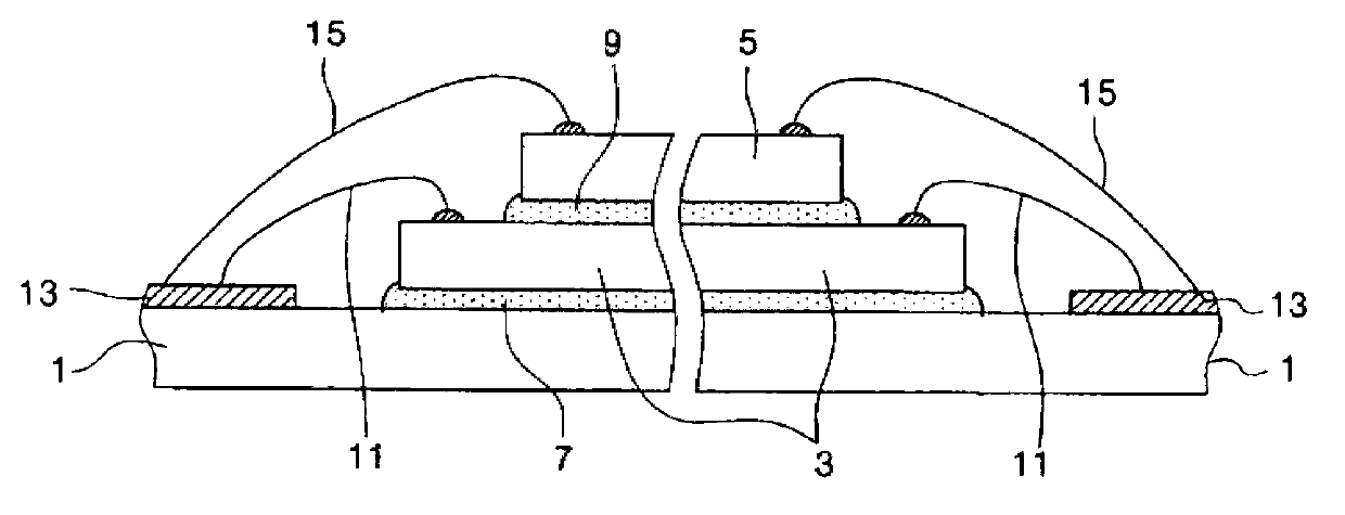
[0029] refer to figure 2 , is a cross-sectional view of the multi-component chip package structure according to the first embodiment of the present invention. In this embodiment, the multi-component chip packaging structure 200 includes a printed circuit board 201 (the first component) on the bottom layer, a chip 204 (the second component) on the printed circuit board 201 , and a chip 204 stacked on the chip 204 chip 205 and inductor 207 (third component). Here, the chip 204, the chip 205 and the inductor 207 are spaced apart from each other and do not touch each other, so as to achieve good electrical isolation. The chip 204 is electrically connected to the printed circuit board 201 through a set of solder balls 202 (first connection structure); the chip 205 and the inductor 207 are electrically connected to the printed circuit board 201 through another set of solder balls 203 located outside the chip 204 .

[0030] Specifically, the chip 205 includes a first straight por...

Embodiment 2

[0036] refer to image 3 , is a cross-sectional view of a multi-component chip package structure according to a second embodiment of the present invention. In this embodiment, the multi-component chip packaging structure 300 includes a lead frame 301 (first component) on the bottom layer, a chip 304 (second component) on the lead frame 301 , and an inductor stacked on the chip 304 306 (third component). Wherein, the chip 304 is connected to the lead frame 301 through a group of bumps 302 (first connection structure).

[0037] The connection between the inductor 306 on the upper layer and the lead frame 301 is realized through the following connection methods:

[0038] The lead frame 301 is arranged in a bent shape, which includes a second straight portion 301-1 and a second bent portion 301-2; the second bent portion 301-2 is located in the outer area of ​​the chip 304 and is separated from the chip 304, Its first end is connected to the second straight line portion 301 - 1...


PUM


Abstract

The invention relates to a chip packaging structure of a plurality of assemblies. The chip packaging structure comprises a first assembly located at the bottom layer, at least one second assembly located above the first assembly and at least one third assembly stacked above the second assemblies. The second assemblies are arranged at intervals and do not contact with each other, the third assemblies are located on the outer sides of the second assemblies, the third assemblies and the third assemblies and the second assemblies are separated from each other and do not contact, each second assembly is electrically connected with the first assembly through a first group of protruding structures, and the third assemblies are electrically connected to the first assembly through a second group of protruding structures outside the second assemblies.

Description

technical field [0001] The present invention relates to semiconductor packaging, and more particularly to a chip packaging structure comprising a plurality of components. Background technique [0002] With the increasing demand for miniaturization, light weight and multi-functionalization of electronic components, the requirements for semiconductor packaging density are getting higher and higher, so as to achieve the effect of reducing the packaging volume. Therefore, the multi-chip packaging structure has become a new hot spot. However, in a multi-chip semiconductor package structure, the connection method between chips has a crucial impact on the size and performance of the semiconductor package. [0003] figure 1 Shown is a cross-sectional view of a multi-chip packaging structure in the prior art. In this implementation, the lower chip 3 and the upper chip 5 are stacked and arranged on the printed circuit board 1 . One surface of the lower chip 3 is connected to the u...

Claims


Application Information

Patent Timeline
IPC IPC(8): H01L23/495
CPCH01F27/00H01L2224/48091H01L23/4951H01L2224/73265H01L2224/32145H01L2224/48465H01L2224/73253H01L2924/30107H01L23/495H01L2924/00014H01L2924/00
Inventor 谭小春叶佳明
Owner HEFEI SMAT TECH CO LTD
Why Eureka
Try Eureka