Crosslinked composition
A composition and cross-linking technology, applied in the direction of nanotechnology, electrical components, nanotechnology, etc., can solve the problems of inability to obtain high photoelectric effect, low conductivity of organic semiconductors, and low photoelectric conversion rate
- Summary
- Abstract
- Description
- Claims
- Application Information
AI Technical Summary
Problems solved by technology
Method used
Image

Examples
Embodiment 1
[0332] (1) Preparation of composition (coating composition)
[0333] Put 16.2mg of 1,3,5-triformylbenzene (manufactured by Nard Laboratories Co., Ltd.) and 29.0mg of tris(4-aminophenyl)amine in a 6ml sample bottle, and dissolve in N,N-dimethylethyl Amide 860mg. The solution was filtered with a filter having a pore size of 0.2 μm to prepare a composition (coating composition).
[0334] (2) Production of organic semiconductor film
[0335] Using the composition obtained in the above step (1), a thin film was formed by spin coating on a substrate, and then heat-treated at 300°C for 1 hour in a nitrogen atmosphere to obtain an organic semiconductor film (hereinafter referred to as BTA- TAPA).
[0336] (3) Structure of organic semiconductor film
[0337] (3-1) Solubility relative to organic solvents
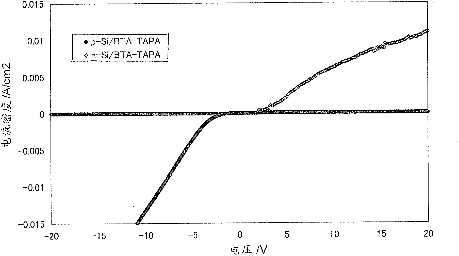
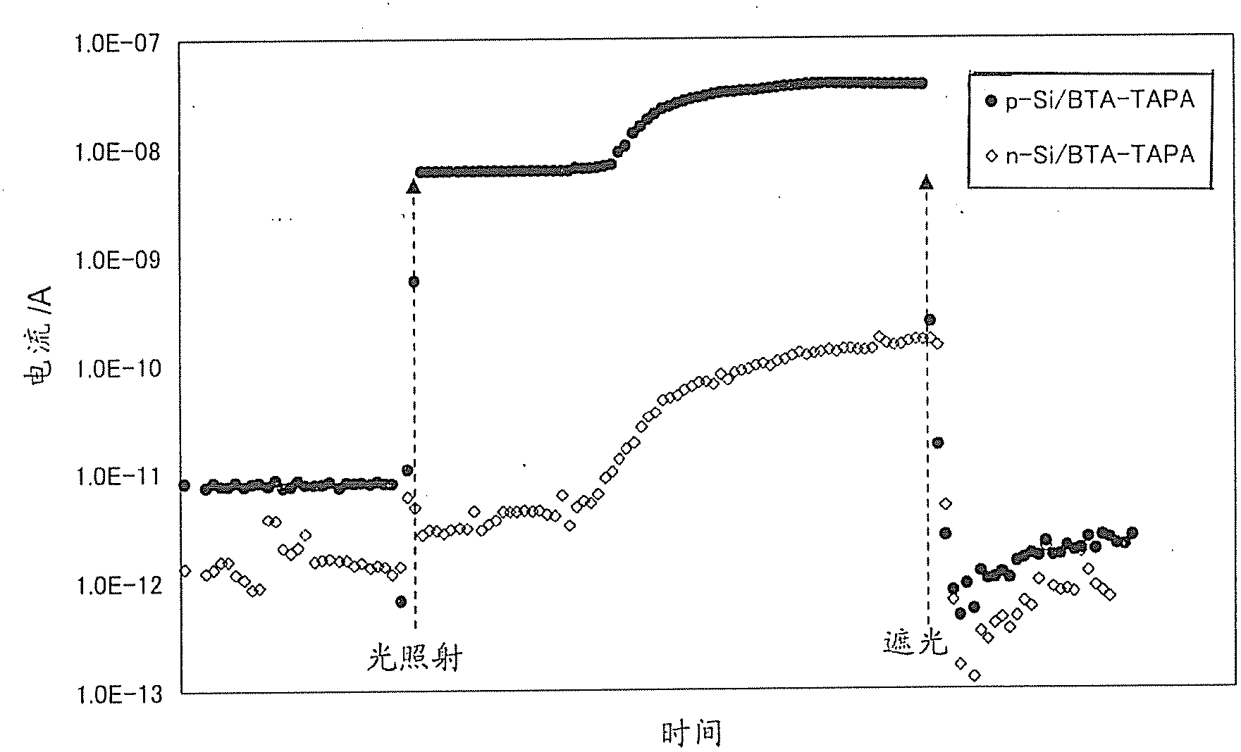
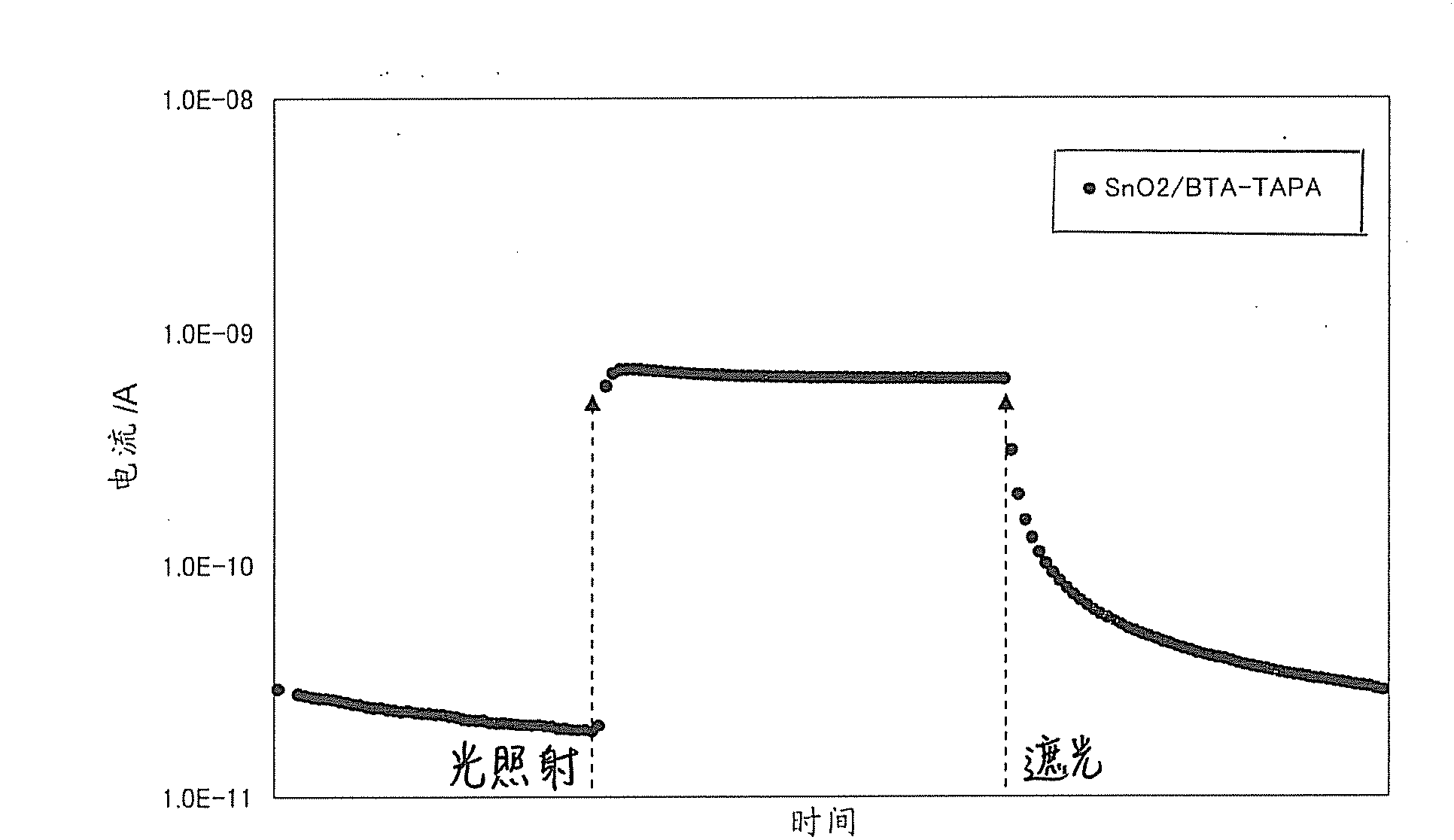
[0338] A silicon wafer (or glass plate) is used as the base material, and the BTA-TAPA film is produced by the method (2) above. Since the film was insoluble in N,N-dimethylacetamide, it was...
Embodiment 2
[0351] (1) Preparation of composition (coating composition)
[0352] Put 16.2mg of 1,3,5-triformylbenzene (manufactured by Nard Laboratories Co., Ltd.) and 29.4mg of 2,7-diaminofluorene in a 6ml sample bottle and dissolve in 1400mg of N,N-dimethylacetamide . The solution was filtered with a filter having a pore size of 0.2 μm to prepare a composition (coating composition).
[0353] (2) Production of organic semiconductor film
[0354] Using the composition obtained in the above step (1), an organic semiconductor film (hereinafter referred to as BTA-DAF) was obtained by the same method as in Example 1.
[0355] (3) Structure of organic semiconductor film
[0356] (3-1) Solubility relative to organic solvents
[0357] The BTA-DAF film was produced by the same method as in Example 1. The film was insoluble in N,N-dimethylacetamide, and therefore, it was confirmed that a three-dimensional network structure was formed.
[0358] (3-2) Band gap
[0359] The UV-Vis spectrum of the BTA-DAF film ...
Embodiment 3
[0367] (1) Preparation of composition (coating composition)
[0368] Put 16.2mg of 1,3,5-triformylbenzene (manufactured by Nard Laboratories Co., Ltd.) and 34.8mg of 1,3-diaminopyrene in a 6ml sample bottle and dissolve in 1650mg of N,N-dimethylacetamide . The solution was filtered with a filter having a pore size of 0.2 μm to prepare a composition (coating composition).
[0369] (2) Production of organic semiconductor film
[0370] Using the composition obtained in the above step (1), an organic semiconductor film (hereinafter referred to as BTA-13DAPy) was obtained by the same method as in Example 1.
[0371] (3) Structure of organic semiconductor film
[0372] (3-1) Solubility relative to organic solvents
[0373] The BTA-13DAPy film was produced by the same method as in Example 1. The film was insoluble in N,N-dimethylacetamide, and therefore, it was confirmed that a three-dimensional network structure was formed.
[0374] (3-2) Band gap
[0375] The UV-Vis spectrum of the BTA-13DAP...
PUM
| Property | Measurement | Unit |
|---|---|---|
| boiling point | aaaaa | aaaaa |
| thickness | aaaaa | aaaaa |
| thickness | aaaaa | aaaaa |
Abstract
Description
Claims
Application Information
 - R&D
- Intellectual Property
- Life Sciences
- Materials
- Tech Scout
- Unparalleled Data Quality
- Higher Quality Content
- 60% Fewer Hallucinations
Browse by: Latest US Patents, China's latest patents, Technical Efficacy Thesaurus, Application Domain, Technology Topic, Popular Technical Reports.
© 2025 PatSnap. All rights reserved.Legal|Privacy policy|Modern Slavery Act Transparency Statement|Sitemap|About US| Contact US: help@patsnap.com