Method for testing transmission fatigue of wafer

A technology of fatigue and chips, which is applied in the field of semiconductor device manufacturing and testing systems, can solve problems such as incomplete systems, affecting equipment stability, and customer losses, and achieve a more comprehensive system effect

Active Publication Date: 2013-03-06
BEIJING SHUOKE ZHONGKEXIN ELECTRONICS EQUIP CO LTD
View PDF3 Cites 2 Cited by
  • Summary
  • Abstract
  • Description
  • Claims
  • Application Information

AI Technical Summary

Problems solved by technology

[0004] The present invention is aimed at the lack of system and incompleteness of the chip transmission fatigue test in the prior art, which affects the stability of the equipment and may cause heavy losses to customers, and develops a set of chip transmission fatigue test system

Method used


Image

  • Method for testing transmission fatigue of wafer

Examples


Embodiment Construction

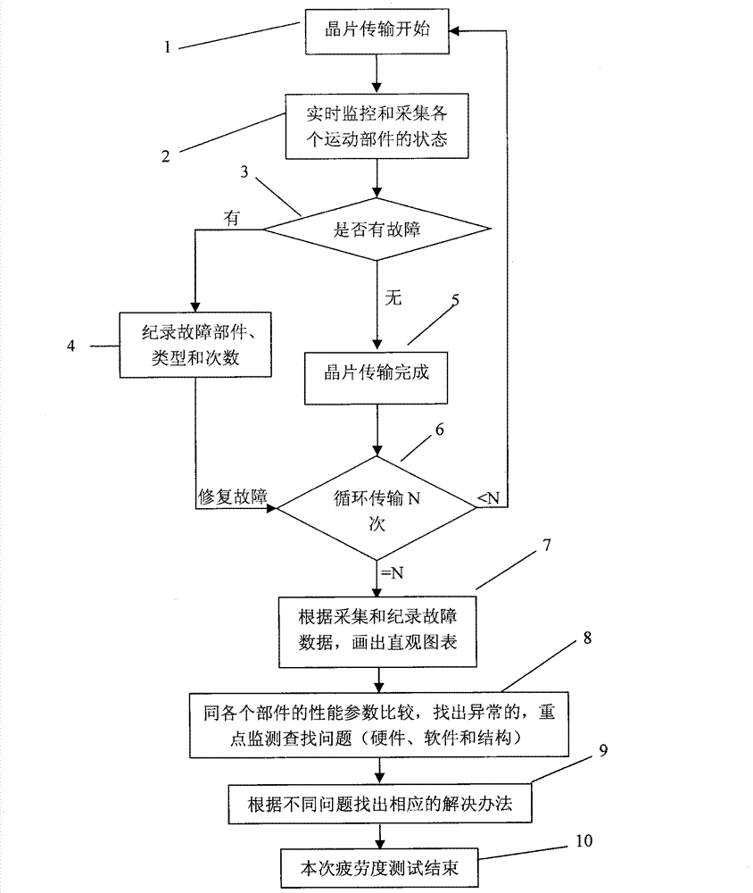
[0011] Attached below figure 1 The present invention will be further described with specific examples, but not as a limitation to the present invention.

[0012] For the wafer transfer fatigue test, the fatigue test method described above was used: figure 1 In this method, more than 4,000 wafers must be transferred every day, and the state data of each component during the transfer process (2) is recorded, mainly including: transfer time, temperature and error of each motor in a period of time, faults during transfer, transfer Number of wafers and number of chips. Make statistics according to the recorded data, and draw them in the form of intuitive graphs (7), which is convenient and easy to understand.

[0013] 1) Draw a graph of the transmission time and the temperature of each motor, and check whether the temperature of the motor fluctuates greatly, and whether the temperature exceeds the factory calibration range. If you find this situation, you should contact the manuf...


PUM


Abstract

The invention discloses a method for testing transmission fatigue of a wafer. The method includes (1), starting transmission of the wafer; (2), monitoring and acquiring states of various moving components in real time; (3), detecting whether faults occur or not; (4), recording faulted components, types of the faulted components and the frequency of the faults; (5), completing transmission of the wafer; (6), repeating transmission by N times; (7), drawing a visual chart according to the acquired and recorded faults; (8), comparing performance parameters of the various components, finding out abnormal performance parameters and monitoring the abnormal performance parameters in a focused manner to find out problems; (9), finding out corresponding solutions according to the different problems; and (10), completing the fatigue test. The method has the advantages that state trends of the various components during long-term movement can be comprehensively reflected, are visible, are easy to understand and bring convenience for statistics, unstable factors can be found out quickly, and the solutions for the problems can be found out pertinently according to classifications of types of the problems.

Description

technical field [0001] The invention relates to a semiconductor device manufacturing and testing system, in particular to a method for testing the fatigue degree of ion implanter wafer transmission. Background technique [0002] An ion implanter is a device that changes the conductivity of the wafer by guiding impurities to be implanted into the semiconductor wafer. The stability of the wafer transfer system is directly related to the production efficiency of the equipment and the benefits of the enterprise. Therefore, a set of effective wafer transfer fatigue The degree of testing method is very important. In the early "marathon" tape-out fatigue test, only by exposing all the problems as much as possible can we provide customers with a stable and safe device. [0003] In view of the importance of the wafer transfer fatigue test, how to develop a systematic and comprehensive wafer transfer fatigue test system is an urgent problem to be solved in the ion implanter stability ...

Claims


Application Information

Patent Timeline
Patent Type & Authority Applications(China)
IPC IPC(8): H01L21/66
Inventor 杨亚兵周文龙谢均宇
Owner BEIJING SHUOKE ZHONGKEXIN ELECTRONICS EQUIP CO LTD
Why Eureka
Try Eureka