Driving method and driving circuit of liquid crystal panel and liquid crystal display device

A technology of a liquid crystal panel and a driving method, applied in static indicators, instruments, etc., can solve the problems of increasing cost and occupying space on the edge of the glass, and achieve the effect of ensuring the duration and quality

Active Publication Date: 2015-04-22
TCL CHINA STAR OPTOELECTRONICS TECH CO LTD
View PDF9 Cites 0 Cited by
  • Summary
  • Abstract
  • Description
  • Claims
  • Application Information

AI Technical Summary

Problems solved by technology

[0003] The control signals of these scanning driver chips will be transmitted from the printed circuit board PCBA to the glass of the LCD panel through the flexible circuit board of the data chip, and then transmitted to the scanning driver chip through the glass wiring. At present, the mainstream design of the LCD panel is narrow bezel. In terms of development, the cost of adding a signal is that an extra line needs to be run on the glass, which will occupy the space on the edge of the glass. In addition, the timing control chip T-CON (timing controller) also needs an additional control signal, and the cost will also increase.

Method used


Image

  • Driving method and driving circuit of liquid crystal panel and liquid crystal display device
  • Driving method and driving circuit of liquid crystal panel and liquid crystal display device
  • Driving method and driving circuit of liquid crystal panel and liquid crystal display device

Examples


example 1

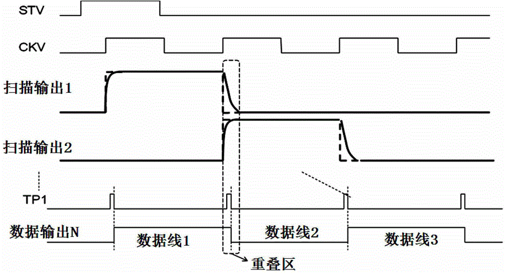
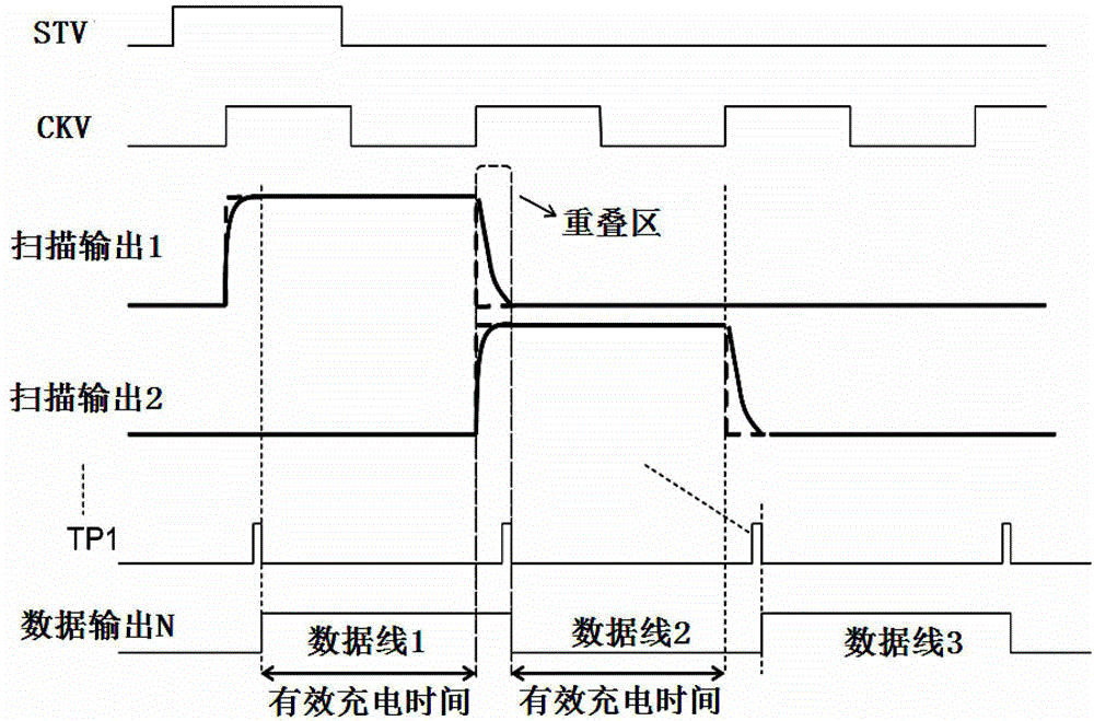
[0049] The sum of the delay time of the timing module and the duration of the data start signal is equal to the time of the overlapping area; the data start chip outputs the data line driving signal at the falling edge of the data start signal. This implementation mode is a technical solution for data output triggered by falling edges, which can ensure that the data is output just after passing the overlapping area, so that the duration of the data signal can be guaranteed to the maximum extent on the premise of avoiding data overlapping in the overlapping area , so that the liquid crystal molecules can have more time to deflect and maintain the corresponding angle to ensure the quality of the display.

example 2

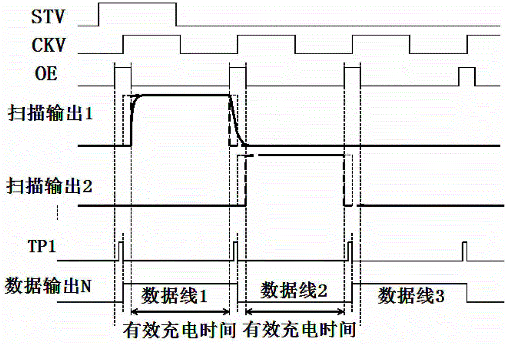
[0051] The delay time of the timing module is not less than the time of the overlapping area; the data start chip outputs the data line driving signal at the rising edge of the data start signal. This implementation mode is a technical solution for triggering data output by a rising edge, which can ensure that the data is output just after passing the overlapping area, so that the duration of the data signal can be guaranteed to the maximum extent on the premise of avoiding data overlapping in the overlapping area , so that the liquid crystal molecules can have more time to deflect and maintain the corresponding angle to ensure the quality of the display.


PUM


Abstract

A drive method and drive circuit for a liquid crystal panel and a liquid crystal display device. The drive method for a liquid crystal panel includes a scan drive process and a data drive process. In the scan drive process, an overlap region turned on at the same time is formed in the middle of switching drive of a previous row of scan line to drive of a next row of scan line. In the data drive process, after a data signal corresponding to the previous row of scan line is sustained to the end of the overlap region, a data signal corresponding to the next row of scan line is output.

Description

technical field [0001] The invention relates to the field of liquid crystal display, and more specifically, relates to a driving method of a liquid crystal panel, a driving circuit and a liquid crystal display device. Background technique [0002] The LCD panel includes criss-cross scanning lines and control lines. The data lines are controlled by the data driver chip. After the data chip receives the data start signal TP1 (latched pulse), it will output the data voltage to the data line of the panel at the falling edge; scan The lines are controlled by scanning driver chips arranged on both sides of the LCD panel. At present, there are 3 control signals required by the scan driver chip to control the opening and closing of each line of the liquid crystal display, namely the start pulse signal STV (start voltage pulse), which controls the beginning of the first line; the clock pulse signal CKV (clock voltage pulse), It is provided to the shift register of the scanning drive...

Claims


Application Information

Patent Timeline
Patent Type & Authority Patents(China)
IPC IPC(8): G09G3/36
CPCG09G2310/0251G09G2320/0233G09G2310/08G09G3/3677G09G2320/0223
Inventor 郭东胜
Owner TCL CHINA STAR OPTOELECTRONICS TECH CO LTD
Why Eureka
Try Eureka