
Pixel circuit and display device

A technology of pixel circuits and sub-circuits, applied in the field of organic light-emitting, can solve the problems of uneven image brightness, uneven backplane current, etc.

Inactive Publication Date: 2013-03-06
BOE TECH GRP CO LTD
View PDF12 Cites 10 Cited by
  • Summary
  • Abstract
  • Description
  • Claims
  • Application Information

AI Technical Summary

Problems solved by technology

When the same driving signal is applied to each pixel, the current flowing through each OLED in the backplane display area is not equal, resulting in uneven current on the backplane, resulting in uneven brightness of the image

Method used


Image

  • Pixel circuit and display device
  • Pixel circuit and display device
  • Pixel circuit and display device

Examples


Embodiment Construction

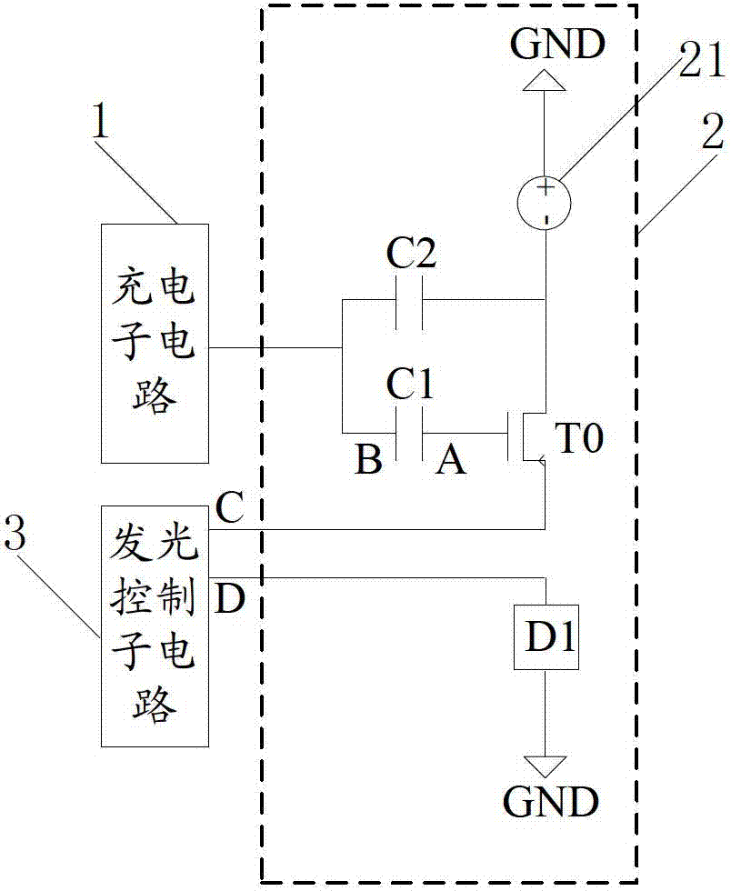
[0018] Embodiments of the present invention provide a pixel circuit and a display device, which are used to improve the uniformity of image brightness in a display area of ​​the display device.

[0019] The driving transistor in the pixel circuit in the embodiment of the present invention may be a thin film transistor (Thin Film Transistor, TFT) or a metal oxide semiconductor field effect transistor (Metal Oxid Semiconductor, MOS). The driving transistor may be an n-type transistor or a p-type transistor.

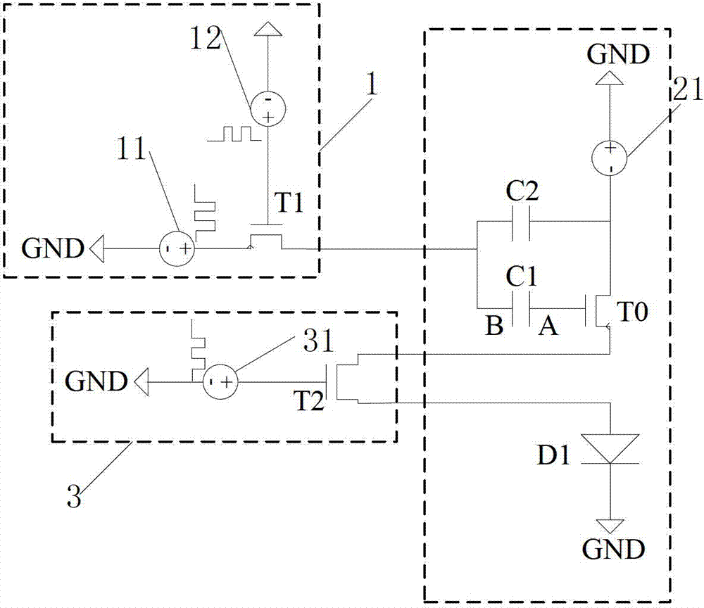
[0020] The light-emitting device described in the embodiment of the present invention may be an organic light-emitting diode (OLED) or an organic electroluminescent element (EL). In the light-emitting phase of the pixel circuit, the driving sub-circuit is turned on, and the light-emitting device realizes light-emitting display under the action of the leakage current of the n-type driving transistor or the p-type driving transistor. The pixel circuit provided by the embodim...


PUM


Abstract

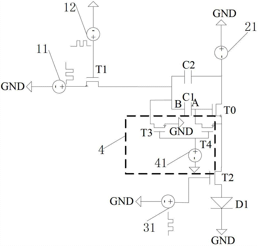
The embodiment of the invention provides a pixel circuit and a display device, which are used for improving the uniformity of the display region image brightness of the display device. The pixel circuit comprises a charging sub circuit, a driving sub circuit and a luminescence control sub circuit, and the driving sub circuit comprises a reference signal source, a driving transistor, a first capacitor, a second capacitor and a luminescent device, wherein a grid electrode of the driving transistor is connected with the first end of the first capacitor, a source electrode of the driving transistor is connected with the output end of the reference signal source, a drain electrode of the driving transistor is connected with the first end of the luminescence control sub circuit, the luminescent control device is connected with the second end of the luminescence control sub circuit, one end of the second capacitor is connected with the second end of the first capacitor, the other end of the second capacitor is connected with the output end of the reference signal source, and the charging sub circuit is connected with the second end of the first capacitor.

Description

technical field [0001] The present invention relates to the field of organic light emitting technology, in particular to a pixel circuit and a display device. Background technique [0002] Organic Light Emitting Diode (OLED) displays have attracted much attention due to their advantages of low power consumption, high brightness, low cost, wide viewing angle, and fast response, and have been widely used in the field of organic light emitting technology. [0003] In OLED displays, there are the following unavoidable problems. First of all, each transistor used to realize image display on the backplane has structural inhomogeneity in the manufacturing process, as well as inhomogeneity in electrical performance and stability, resulting in the threshold voltage V of the transistor. th A drift has occurred. Second, transistors suffer from reduced stability when turned on for long periods of time. In addition, with the development of OLED size enlargement, the load on the signal...

Claims


Application Information

Patent Timeline
Patent Type & Authority Applications(China)
IPC IPC(8): G09G3/32G09G3/3258
Inventor 马占洁
Owner BOE TECH GRP CO LTD
Learn More