
Display Device and Display Method Thereof

a display device and display method technology, applied in the field of display technology, can solve problems such as discomfort for viewers, and achieve the effect of avoiding color shift and avoiding discomfort for viewers

Active Publication Date: 2015-06-04
SHENZHEN CHINA STAR OPTOELECTRONICS TECH CO LTD
View PDF5 Cites 12 Cited by
  • Summary
  • Abstract
  • Description
  • Claims
  • Application Information

AI Technical Summary

Benefits of technology

This patent is for a new display device and method that solves the problem of color distortion in a big viewing angle and ensures the left and right eye images are equally bright when displayed in 3D mode. This makes the viewing experience more comfortable for the viewer.

Problems solved by technology

As a result, luminance of the sub area 102 visible to left and right eyes of a viewer respectively is always different, causing uncomfortable to the viewer.

Method used


Image

  • Display Device and Display Method Thereof
  • Display Device and Display Method Thereof
  • Display Device and Display Method Thereof

Examples


first embodiment

[0039]Please refer to FIG. 2, a circuit diagram of a sub-pixel unit of a display device according to the present invention.

[0040]The display device displays two-dimensional and three-dimensional images, and switches from three-dimensional display mode to two-dimensional display mode when needed, and likewise, switches from two-dimensional display mode to three-dimensional display mode. The display device comprises a display panel comprising one or more pixel units, each of which comprises one or more sub-pixel unit.

[0041]The sub-pixel unit comprises a first sub-pixel area 204, a second sub-pixel area 205, a first Thin Film Transistor (TFT) 206, a second TFT 207, a capacitor 208 and a switch unit.

[0042]The first TFT 206 connects to a first scan line 202, a data line 201, and the first sub-pixel area 204. The second TFT 207 connects to the first scan line 202, the first data line 201 and the second sub-pixel area 205. The capacitor 208 receives electrical charge of the second sub-pixe...

second embodiment

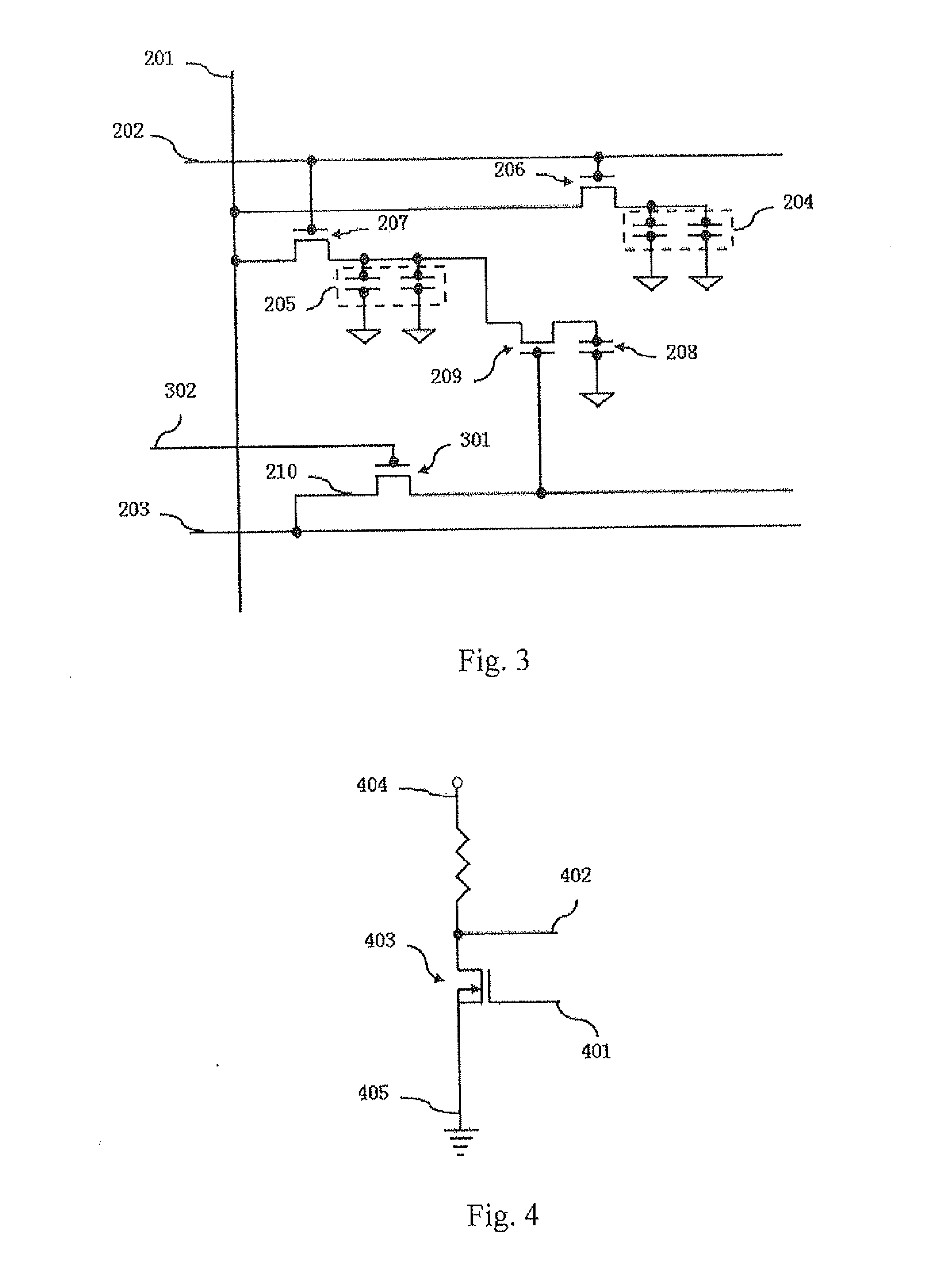
[0048]Please refer to FIG. 3, a circuit diagram of a sub-pixel unit of the display device according to the present invention. The embodiment is similar with the foregoing embodiment, except for the following differences:

[0049]In the embodiment, the switch also comprises a fourth TFT 301, which receives a second control signal and the first control signal and sends the first control signal to the third TFT 209 according to the second control signal.

[0050]The fourth TFT 301 comprises a fourth drain, a fourth source and a fourth gate.

[0051]The fourth gate receives the second control signal to turns on and off a second current channel between the fourth drain and the fourth source. The third TFT 209 connects to the fourth drain, and the fourth source connects to the second scan line 203 of the display panel; or, the third TFT 209 connects to the fourth source, and the fourth drain connects to the second scan line 203 of the display panel.

[0052]In the embodiment, the second control signa...


PUM


Abstract

A display device and a method for displaying image are proposed. The first TFT and the second TFT are connected to a scan line and a data line. The first TFT and the second TFT are connected to a first sub-pixel area and a second sub-pixel area respectively. A switch unit is used for turning on / off a first current channel when the display panel is under 2D / 3D display mode. The display device of the present disclosure avoids color shift in a large viewing angle under two-dimensional display mode, and displays identical luminance of left eye and right eye images under three-dimensional display mode, avoiding uncomfortable to the viewer.

Description

BACKGROUND OF THE INVENTION[0001]1. Field of the Invention[0002]The present invention relates to a display technology field, more particularly, to a display device and a display method thereof.[0003]2. Description of the Prior Art[0004]To solve a problem of color shift in a large viewing angle, conventional display devices usually apply Low Color Shift (LCS) technology, more particularly, dividing a sub-pixel unit 100 of a pixel unit into a main area 101 and a sub area 102. As FIG. 1 indicates, the main area 101 and the sub area 102 are applied with respective driving voltages to generate different luminance, so that luminance deviation of the pixel unit is not significant in different viewing angles.[0005]The inventor finds a practical problem of conventional arts as follow:[0006]when the sub area 102 is in a moment between two frames with different polarities, greater voltage drop applied on the sub area 102 causes greater luminance variety; when the sub area 102 is in a moment be...

Claims


Application Information

Patent Timeline
IPC IPC(8): G06T1/00G09G5/00H04N13/04
CPCG06T1/00G09G2300/0443G09G5/006H04N13/0497G09G3/003G09G3/3659H04N13/359H04N13/398
Inventor WU, YUFU, WEI
Owner SHENZHEN CHINA STAR OPTOELECTRONICS TECH CO LTD
Learn More